 | –≠–ª–µ–∫—Ç—Ä–æ–Ω–Ω—ã–π –∫–æ–º–ø–æ–Ω–µ–Ω—Ç: CHA2293 | –°–∫–∞—á–∞—Ç—å:  PDF PDF  ZIP ZIP |
CHA2293
Ref. : DSCHA22931201 -20-July-01
1/7
Specifications subject to change without notice
Route DÈpartementale 128 , B.P.46 - 91401 ORSAY Cedex - FRANCE
Tel.: +33 (0)1 69 33 03 08 - Fax : +33 (0)1 69 33 03 09
24.5-29.5GHz Low Noise, Variable Gain Amplifier
GaAs Monolithic Microwave IC
Description
The CHA2293 is a high gain four-stage
monolithic low noise amplifier with variable gain.
It is designed for a wide range of applications,
from military to commercial communication
systems.The backside of the chip is both RF and
DC grounded. This helps simplify the assembly
process.
The circuit is manufactured with a PM-HEMT
process, 0.25µm gate length, via holes through
the substrate, air bridges and electron beam
gate lithography.
It is available in chip form.
Main Features
∑
Frequency range : 24.5-29.5GHz
∑
3dB Noise Figure.
∑
24dB gain
∑
Gain control range: 15dB
∑
Low DC power consumption, 160mA @ 5V
∑
Chip size : 2.32 X 1.23 X 0.10 mm
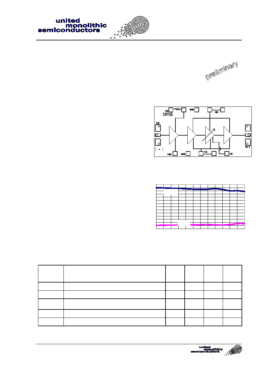
Typical on wafer measurements :Gain & NF
0
2
4
6
8
10
12
14
16
18
20
22
24
26
28
24
25
26
27
28
29
30
Frequency (GHz)
Gain (dB)
NF (dB)
Main Characteristics
Tamb. = 25∞C
Parameter Min
Typ
Max
Unit
Fop
Operating frequency range
24.5
29.5
GHz
G Small
signal
gain
24 dB
NF Noise
figure
3 3.5 dB
Gctrl
Gain control range with Vc variation
15
dB
Id Bias
current
150 mA
ESD Protection : Electrostatic discharge sensitive device. Observe handling precautions !
V5 Vd
Vg1 Vg Vc

24.5-29.5GHz LNA VGA
CHA2293
Ref. : DSCHA22931201 -20-July-01
2/7
Specifications subject to change without notice
Route DÈpartementale 128 , B.P.46 - 91401 ORSAY Cedex - FRANCE
Tel.: +33 (0)1 69 33 03 08 - Fax : +33 (0)1 69 33 03 09
Electrical Characteristics for Broadband Operation
Tamb = +25∞C, V5=Vd= 5V
Symbol Parameter Min
Typ
Max
Unit
Fop
Operating frequency range
24.5
29.5
GHz
G
Small signal gain (1)
24
dB
G
Small signal gain flatness (1)
±1.5
dB
Is
Reverse isolation (1)
50
dB
NF
Noise figure with Vc=1.2V
3
3.5
dB
Gctrl
Gain control range versus Vc
15
dB
P1dB
Output power at 1dB compression with Vc=1.2V
12
dBm
VSWRin Input
VSWR
(1)
4.0:1
VSWRout Output
VSWR
(1)
2.0:1
Vd
DC voltage
V5= Vd
Vc
-1.5
5
[-0.7, 1.2]
1.3
V
V
Id1
Bias current (2) with Vc=1.2V
35
mA
Id
Bias current total (3) with Vc=1.2V
160
mA
(1) These values are representative of on-wafer measurements that are made without bonding
wires at RF ports.
(2) For optimum noise figure, the bias current Id1 should be adjust to 35mA with Vg1 voltage.
(3) With Id1=35mA, adjust Vg voltage for a total drain current around 160mA.
Absolute Maximum Ratings
Tamb. = 25∞C (1)
Symbol Parameter
Values
Unit
Vd Drain
bias
voltage
5.5
V
Vc Control
bias
voltage
1.5
V
Id Drain
bias
current
250
mA
Vg
Gate bias voltage
-2.0 to +0.4
V
Pin
Maximum peak input power overdrive (2)
+15
dBm
Ta
Operating temperature range
-40 to +85
∞C
Tstg
Storage temperature range
-55 to +155
∞C
(1) Operation of this device above anyone of these parameters may cause permanent damage.
(2) Duration < 1s.

24.5-29.5GHz LNA VGA
CHA2293
Ref. : DSCHA22931201 -20-July-01
3/7
Specifications subject to change without notice
Route DÈpartementale 128 , B.P.46 - 91401 ORSAY Cedex - FRANCE
Tel.: +33 (0)1 69 33 03 08 - Fax : +33 (0)1 69 33 03 09
Typical on wafer Measurements
Bias Conditions :
V5=Vd= 5 Volt, Vg1 pour Id1= 35mA, Vg = -0.3V, Vc=1.2V
0
2
4
6
8
10
12
14
16
18
20
22
24
26
28
24
25
26
27
28
29
30
Frequency (GHz)
Gain (dB)
NF (dB)
Gain & Noise Figure versus frequency
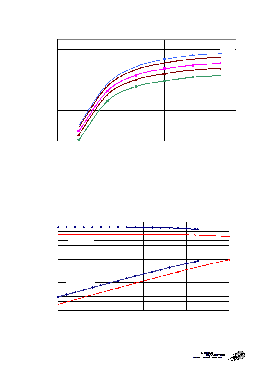
Bias Conditions :
V5=Vd= 5 Volt, Vg1 =Vg = -0.3V
0
5
10
15
20
25
30
24
25
26
27
28
29
30
Frequency (GHz)
(dB
)
Vc=1.2V
Vc=-0.5V
Control gain range versus frequency
24.5-29.5GHz LNA VGA
CHA2293
Ref. : DSCHA22931201 -20-July-01
4/7
Specifications subject to change without notice
Route DÈpartementale 128 , B.P.46 - 91401 ORSAY Cedex - FRANCE
Tel.: +33 (0)1 69 33 03 08 - Fax : +33 (0)1 69 33 03 09
10
14
18
22
26
30
-1
-0.5
0
0.5
1
1.5
Control voltage Vc (V)
(d
B)
24GHz
30GHz
29GHz
28GHz
26GHz
Gain versus control voltage
In jig Measurements
Bias Conditions :
V5=Vd= 5 Volt, Vg1= Vg = -0.3V, Vc= 1.2V
All these measurement include the losses from the jig ( about 0.5dB on gain, 0.2dB on noise
figure and 0.3dB on output power).
-8
-6
-4
-2
0
2
4
6
8
10
12
14
16
18
20
22
24
26
28
30
-30
-25
-20
-15
-10
Input power (dBm)
Gain (dB)
Pout (dBm)
Gain & Output power @ 24-26 GHz

24.5-29.5GHz LNA VGA
CHA2293
Ref. : DSCHA22931201 -20-July-01
5/7
Specifications subject to change without notice
Route DÈpartementale 128 , B.P.46 - 91401 ORSAY Cedex - FRANCE
Tel.: +33 (0)1 69 33 03 08 - Fax : +33 (0)1 69 33 03 09
-10
-8
-6
-4
-2
0
2
4
6
8
10
12
14
16
18
20
22
24
26
-30
-25
-20
-15
-10
Input power (dBm)
Gain (dB)
Pout (dBm)
Gain & Output power @ 28≠30 GHz
0
2
4
6
8
10
12
14
16
18
20
23
25
27
29
31
Frequency ( GHz)
N
o
i
s
e Fi
gur
e (dB)
-10
-6
-2
2
6
10
14
18
22
26
30
Ga
i
n
(d
B
)
NF
G
a
i
n
Vc= +1.2V
Vc= +0.8V
Vc= 0V
Vc= -0.4V
Gain & Noise Figure versus Vc