CHA3063
Ref : DSCHA30633273 - 30 Sep 03
1/7
Specifications subject to change without notice
United Monolithic Semiconductors S.A.S.
Route DÈpartementale 128 - B.P.46 - 91401 Orsay Cedex France
Tel. : +33 (0)1 69 33 03 08 - Fax : +33 (0)1 69 33 03 09
5.5-23GHz Driver Amplifier
GaAs Monolithic Microwave IC
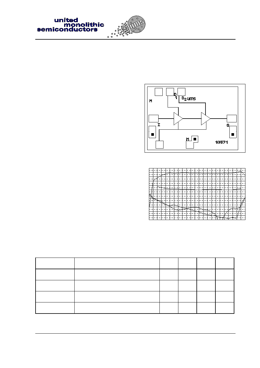
Description
The CHA3063 is a two-stage general
purpose monolithic medium power
amplifier.The backside of the chip is both RF
and DC grounds.This helps simplify the
assembly process.
The circuit is manufactured with a PM-
HEMT process : 0.25µm gate length, via
holes through the substrate, air bridges and
electron beam gate lithography.
It is supplied in chip form.
Main Feature
ß Broad band performance 5.5-23GHz
ß 21dBm output power (Psat)
ß 19dB gain, ± 1dB gain flatness
ß PAE:11%@P-1dB typical
ß
Chip size : 1.33 x 0.910x 0.1mm
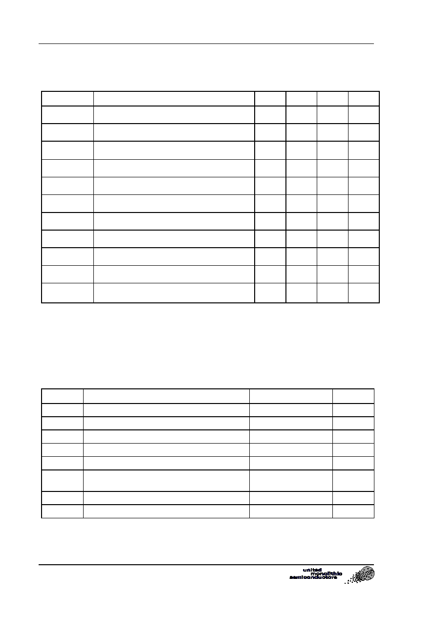
On wafer typical measurements
Main Characteristics
Tamb = +25∞C
Symbol Parameter
Min
Typ
Max
Unit
Fop
Operating frequency range
5.5
23
GHz
G
Small signal gain
18
19
dB
Pout
Output power, Pin=0dBm
+18
+20
dBm
Id_small_signal Bias current
160
210
mA
ESD Protection : Electrostatic discharge sensitive device observe handling precautions !
-24
-20
-16
-12
-8
-4
0
4
8
12
16
20
24
2
4
6
8
10
12
14
16
18
20
22
24
Frequency ( GHz )
G
a
i
n
R
l
o
s
se
s
& N
F
(
d
B
)
NF
dBS21
dBS11
dBS22
CHA3063
5.5-23GHz Driver Amplifier
Ref : DSCHA30633273 - 30 Sep 03
2/7
Specifications subject to change without notice
Route DÈpartementale 128 , B.P.46 - 91401 ORSAY Cedex - FRANCE
Tel.: +33 (0)1 69 33 03 08 - Fax : +33 (0)1 69 33 03 09
Electrical Characteristics on wafer
Tamb = +25∞C, Vd1 = Vd2 =4V Vg tuned for Id=160mA (around ≠0.27V)
Symbol Parameter Min
Typ
Max
Unit
Fop
Operating frequency range
5.5
23
GHz
G
Small signal gain
18
19
dB
G
Small signal gain flatness
±1.0
dB
Is
Reverse isolation
35
dB
P1dB
CW output power at 1dB compression (1)
+16
+18
dBm
Psat
Saturated Output Power (Pin=0dBm)
+18
+21
dBm
IP3
3 rd order intercept(2)
28
dBm
VSWRin
Input VSWR
2.0:1
2.5:1
VSWRout
Output VSWR
2.0:1
2.5:1
NF Noise
figure
4.5 6 dB
Id_
small signal
Bias current
160
210
mA
(1) These values are representative for CW on-wafer measurements that are made without
bonding wires at the RF ports.
(2) Value representative for CW on jig measurement
Absolute Maximum Ratings
Tamb. = 25∞C (1)
Symbol Parameter
Values
Unit
Vds
Drain bias voltage_small signal
5.0
V
Ids
Drain bias current_small signal
210
mA
Vg
Gate bias voltage
-2 to +0.4
V
Ig
Gate bias current
0.7
mA
Vgd
Maximun negative gate drain Voltage (Vg-Vd)
-5
V
Pin
Maximum continuous input power
Maximum peak input power overdrive (2)
+1
+15
dBm
dBm
Ta
Operating temperature range
-40 to +85
∞C
Tstg
Storage temperature range
-55 to +125
∞C
(1) Operation of this device above anyone of these parameters may cause permanent damage.
(2) Duration < 1s.
5.5-23GHz Driver Amplifier
CHA3063
Ref : DSCHA30633273 - 30 Sep 03
3/7
Specifications subject to change without notice
Route DÈpartementale 128 , B.P.46 - 91401 ORSAY Cedex - FRANCE
Tel.: +33 (0)1 69 33 03 08 - Fax : +33 (0)1 69 33 03 09
Typical Scattering Parameters ( On wafer Sij measurements)
Bias Conditions :
Vd1,2= 4V, Vg = -0.27V, Id = 160 mA.
FREQ
S11
S11
S12
S12
S21
S21
S22
S22
GHz
dB
/∞
dB
/∞
dB
/∞
dB
/∞
1,0
-0,3
-35,6
-60,9
84,0
-12,7
86,9
-0,6
-35,0
2,0
-0,7
-75,6
-63,1
142,8
-13,7
-179,2
-1,4
-67,7
3,0
-3,4
-113,7
-54,5
-53,2
11,6
123,1
-4,7
-93,2
4,0
-5,7
-140,7
-53,1
138,2
15,2
58,5
-6,2
-111,6
5,0
-7,9
-170,3
-43,5
67,4
16,4
19,0
-7,4
-133,3
6,0
-9,0
162,5
-44,2
34,7
18,8
-12,3
-11,1
-149,1
7,0
-11,3
121,8
-41,0
13,6
19,3
-46,9
-12,0
-155,1
8,0
-13,5
82,5
-38,7
-16,7
18,9
-75,2
-11,6
-173,2
9,0
-14,3
39,7
-37,6
-39,6
19,1
-100,4
-12,9
171,7
10,0
-14,0
0,9
-37,1
-61,4
19,3
-125,2
-14,4
165,8
11,0
-13,2
-34,0
-36,7
-82,9
19,5
-150,7
-13,7
164,9
12,0
-13,2
-62,6
-35,6
-107,7
19,6
-175,1
-13,5
148,9
13,0
-15,3
-95,8
-36,0
-126,6
19,5
159,3
-11,9
131,3
14,0
-16,7
-125,2
-35,0
-148,4
19,2
133,1
-11,9
116,0
15,0
-21,2
-125,5
-34,7
-175,9
18,5
111,1
-13,1
95,0
16,0
-18,6
-140,0
-36,4
170,4
18,2
89,1
-14,7
79,9
17,0
-19,8
-124,7
-36,4
137,3
18,1
70,4
-19,5
72,4
18,0
-18,8
-172,0
-38,5
135,9
18,1
44,3
-17,4
72,2
19,0
-20,8
101,6
-37,4
154,6
18,0
22,0
-18,5
57,4
20,0
-19,8
23,1
-35,2
125,8
18,0
-2,5
-19,4
47,4
21,0
-15,4
-14,7
-34,0
101,5
18,2
-26,4
-23,3
32,5
22,0
-14,2
-34,2
-33,8
71,7
18,9
-57,7
-21,4
76,8
23,0
-11,5
-43,5
-35,3
46,5
19,5
-89,3
-16,9
77,6
24,0
-11,6
-30,9
-33,1
-0,4
20,4
-144,0
-6,3
46,6
25,0
-3,9
-46,7
-34,9
-86,0
17,6
153,9
-3,1
-13,3
26,0
-2,0
-74,8
-35,3
-172,0
10,9
104,5
-3,2
-59,0
27,0
-1,3
-99,2
-39,7
157,6
3,9
69,9
-4,3
-90,9
28,0
-1,3
-115,8
-33,9
138,6
-3,5
44,6
-4,7
-113,7
29,0
-1,3
-128,4
-32,3
128,4
-12,1
29,3
-5,0
-133,9
30,0
-1,2
-140,1
-28,7
96,4
-21,0
47,7
-5,9
-153,6

CHA3063
5.5-23GHz Driver Amplifier
Ref : DSCHA30633273 - 30 Sep 03
4/7
Specifications subject to change without notice
Route DÈpartementale 128 , B.P.46 - 91401 ORSAY Cedex - FRANCE
Tel.: +33 (0)1 69 33 03 08 - Fax : +33 (0)1 69 33 03 09
Typical ON JIG MEASUREMENTS (deembedded)
Bias Conditions :
Vd1,2= 4V, Vg = -0.27V, Id = 160 mA
GAIN & RLOSS MEASUREMENTS IN TEST JIG
-35
-29
-23
-17
-11
-5
1
7
13
19
25
1
3
5
7
9
11
13
15
17
19
21
23
25
27
FREQ (GHz)
G
a
in/R
losses (dB
)
S21
S11
S22
POWER MEASUREMENTS IN TEST JIG (deembedded)
0
5
10
15
20
25
30
4
6
8
10
12
14
16
18
20
22
24
FREQ (GHz)
OUTPUT POW
E
R (dBm
) / PAE
-5
0
5
10
15
20
25
Gain (dB)
P-1dB
Psat (Glin-3dB)
Linear Gain
PAE @ 1 db compression
5.5-23GHz Driver Amplifier
CHA3063
Ref : DSCHA30633273 - 30 Sep 03
5/7
Specifications subject to change without notice
Route DÈpartementale 128 , B.P.46 - 91401 ORSAY Cedex - FRANCE
Tel.: +33 (0)1 69 33 03 08 - Fax : +33 (0)1 69 33 03 09
Typical ON JIG POWER MEASUREMENTS (deembedded)
Bias Conditions :
Vd1,2= 4V, Vg = -0.27V, Id = 160 mA
FREQ: 6 GHz
0
5
10
15
20
25
-16
-14
-12
-10
-8
-6
-4
-2
0
2
4
Pin (dBm)
Po
u
t
(
d
B
m
)
/ G
a
in
(
d
B
)
/ PA
E (
%
)
0
50
100
150
200
250
300
350
400
450
500
Id
(m
A)
Pout
Gain
Id
PAE
CHA3063
V
d=4V Id=160mA @ 23.5GHz
f=10MH
z
-50
-45
-40
-35
-30
-25
-20
-15
-10
-5
0
5
10
15
20
25
30
35
-16
-14
-12
-10
-8
-6
-4
-2
0
2
4
6
8
10
12
14
Input power (dBm)
Out
put
powe
r
(
d
B
)
-5
5
15
25
35
45
55
65
75
85
I
M
3(
d
B
c)
H3
H1
F2 + ( F2-F1 ) Df=10MHz
F2 Df=10MHz
IM3
IP3 # 28.5dBm
Fundamental
3rd order
IM3
FREQ: 20GHz
0
5
10
15
20
25
-16
-14
-12
-10
-8
-6
-4
-2
0
2
4
Pin (dBm)
Po
u
t
(d
Bm
) / Ga
in
(d
B) / PAE (%
)
0
50
100
150
200
250
300
350
400
450
500
Id
(m
A)
Pout
Gain
Id
PAE