
CHA3092
Ref. :DSCHA30920356 21-Dec.-00
1/
7
Specifications subject to change without notice
United Monolithic Semiconductors S.A.S.
Route DÈpartementale 128 - B.P.46 - 91401 Orsay Cedex France
Tel. : +33 (0)1 69 33 03 08 - Fax : +33 (0)1 69 33 03 09
20-33GHz Medium Power Amplifier
GaAs Monolithic Microwave IC
Description
The CHA3092 is a high gain broadband four-
stage monolithic medium power amplifier. It is
designed for a wide range of applications, from
military to commercial communication
systems. The backside of the chip is both RF
and DC grounds. This helps simplify the
assembly process.
A B.I.T. ( Build In Test ) monitors a DC voltage
that is representative of the microwave output
power.
The circuit is manufactured with a PM-HEMT
process, 0.25µm gate length, via holes through
the substrate, air bridges and electron beam
gate lithography.
It is available in chip form.
Main Features
Broadband performances : 20-33GHz
20dBm output power.
22dB
±
1.0dB gain
Very good broadband input matching
On chip output power level DC detector
Low DC power consumption, 300mA @ 3.5V
Chip size : 0.88 X 1.72 X 0.10 mm
Vg1
Vg2
Vg3,4
Vdet
Vd2,3,4
Vd1
IN
OUT
DI
Typical on wafer measurements :
Input Rloss : solid line & output Rloss : dash line.
Main Characteristics
Tamb. = 25∞C
Symbol
Parameter
Min
Typ
Max
Unit
Fop
Operating frequency range
20
33
GHz
G
Small signal gain
20
22
dB
P03
Output power at 3dB gain compression
20
23
dBm
Id_
small signal
Bias current
300
400
mA
ESD Protection : Electrostatic discharge sensitive device. Observe handling precautions !
CHA3092
20-33GHz Medium Power Amplifier
Ref. : DSCHA30920356 21-Dec.-00
2/
7
Specifications subject to change without notice
Route DÈpartementale 128 , B.P.46 - 91401 ORSAY Cedex - FRANCE
Tel.: +33 (0)1 69 33 03 08 - Fax : +33 (0)1 69 33 03 09
Electrical Characteristics for Broadband Operation
Tamb = +25∞C, Vd1,2,3,4 = 3.5V recommended
Symbol
Parameter
Min
Typ
Max
Unit
Fop
Operating frequency range (1)
20
33
GHz
G
Small signal gain (1)
20
22
dB
G
Small signal gain flatness (1)
±
1.0
dB
Is
Reverse isolation (1)
50
dB
P1dB
Pulsed output power at 1dB compression (1)
18
20
dBm
P03
Output power at 3dB gain compression
20
23
dBm
IP3
3
rd
order intercept point
29
dBm
PAE
Power added efficiency at saturation
10
%
VSWRin
Input VSWR (1)
2.0:1
VSWRout
Output VSWR (1)
3.0:1
NF
Noise figure
10.0
dB
Vdet
Detected voltage: at 26GHz @ Pout=20dBm (2)
1
V
Id_
small signal
Bias current
300
400
mA
(1) These values are representative for pulsed on-wafer measurements that are made without
bonding wires at the RF ports. In the case of a jig or a module CW mode operation, the typical
output power may be around 2dB less.
(2) Voltage across an external 10kOhm parallel resistor connected to the voltage detector pad.
Absolute Maximum Ratings
Tamb. = 25∞C (1)
Symbol
Parameter
Values
Unit
Vds
Drain bias voltage_small signal (2)
4.0
V
Ids
Drain bias current_small signal
400
mA
Vgs
Gate bias voltage
-2 to +0.4
V
Vdg
Negative Drain Gate voltage (= Vds ≠ Vgs)
+5
V
Pin
Maximum continuous input power (2)
Maximum peak input power overdrive (3)
+4
+15
dBm
dBm
Ta
Operating temperature range
-40 to +85
∞C
Tstg
Storage temperature range
-55 to +155
∞C
(1) Operation of this device above anyone of these parameters may cause permanent damage.
(2) 3.5V recommended for up to a max of 3dB gain compression.
(3) Duration < 1s.

20-33GHz Medium Power Amplifier
CHA3092
Ref. : DSCHA30920356 21-Dec.-00
3/
7
Specifications subject to change without notice
Route DÈpartementale 128 , B.P.46 - 91401 ORSAY Cedex - FRANCE
Tel.: +33 (0)1 69 33 03 08 - Fax : +33 (0)1 69 33 03 09
Typical Scattering Parameters ( On wafer Sij measurements )
Bias Conditions :
Vd1,2,3,4 = 3.5 Volt, Vg1,2,3,4 = -0.15 Volt, Id = 300 mA.
Freq.
GHz
S11
dB
S11
/
/
/
/
∞
S12
dB
S12
/
/
/
/
∞
S21
dB
S21
/
/
/
/
∞
S22
dB
S22
/
/
/
/
∞
10
-17.1
134.5
-62.3
-143
4.8
144.2
-5.2
-173.7
11
-17.6
138.2
-62.8
137
9
112.4
-6.3
179.4
12
-18.1
140.3
-78.5
-31
13
78.1
-7.3
173.5
13
-18.9
138
-59.9
157.3
16.5
41.6
-8.2
168.7
14
-19
141.5
-62.4
126.9
19.1
2.9
-9.1
170.5
15
-19.2
138
-65.1
-160.1
21.1
-35.2
-8.7
171.3
16
-19.8
137.8
-64.3
157.5
22.1
-74.3
-9.3
165.6
17
-20.9
138.8
-60.3
-178.9
22.3
-110.1
-9.2
162.4
18
-20.1
146.2
-67.6
138.4
23.9
-137
-9.1
145.5
19
-20.4
131.7
-54.2
100.1
22.3
-175.3
-13.6
161.1
20
-24.3
126.9
-58.8
3.5
22.8
163.8
-10.9
154.2
21
-25.1
144.6
-62.5
-138.8
22.8
134.4
-12.7
148.6
22
-25.2
148
-60.5
156
22.7
109.3
-14
155.7
23
-24
157.7
-55.6
142.2
22.6
87.4
-13.9
154.7
24
-27.7
157.3
-63.7
135.9
22.9
61.6
-14.3
160.8
25
-28.7
-178.8
-57.1
126.6
22.8
36.7
-13.8
170.2
26
-28.5
-161.1
-55.7
96.9
22.9
15.5
-12.6
167.1
27
-23
-151.3
-66
72.7
23
-10.2
-13.1
161.9
28
-22.1
-157.5
-59.1
125.1
22.8
-33.6
-12.5
162.5
29
-20.7
-167.6
-56.6
85.1
22.7
-57.2
-12.1
158.2
30
-20
-175.2
-57
106.5
22.3
-80.4
-11.8
149.7
31
-20.8
171.5
-57
97.8
22.2
-101.9
-11.9
144.9
32
-21.1
168
-52
77.7
22.2
-125.3
-13.2
130.1
33
-21.3
166.5
-52.5
62.7
21.9
-150.2
-13
134.1
34
-22
155.6
-51.2
75
21.4
-174.1
-13.1
124
35
-23
140.2
-52.7
76.7
20.8
164.1
-13.8
113.6

CHA3092
20-33GHz Medium Power Amplifier
Ref. : DSCHA30920356 21-Dec.-00
4/
7
Specifications subject to change without notice
Route DÈpartementale 128 , B.P.46 - 91401 ORSAY Cedex - FRANCE
Tel.: +33 (0)1 69 33 03 08 - Fax : +33 (0)1 69 33 03 09
Typical On wafer Power Measurements
Bias Conditions :
Vd1,2,3,4 = 3.5 Volt, Vg1,2,3,4 = -0.15 Volt, Id = 300 mA.
On wafer Pin / Pout at 20 GHz
15
16
17
18
19
20
21
22
23
24
25
-3
-2
-1
0
1
2
3
4
5
Pin ( dBm )
Pout
( dBm
)
0
3
6
9
12
15
18
21
24
27
30
P.
A.
E
.
( % )
On wafer Pin / Pout at 22 GHz
15
16
17
18
19
20
21
22
23
24
25
-3
-2
-1
0
1
2
3
4
5
Pin ( dBm )
Pout
( dBm
)
0
3
6
9
12
15
18
21
24
27
30
P.
A.
E
.
( % )
Notes :
1- Test conditions :
Vd1,2,3,4 = 3.5 Volt, Vg1,2,3,4 = -0.15 Volt.
2- Power measurements are typical
( solid lines ).
P.A.E. is representative of on wafer
measurements on a typical circuit
( Dotted lines ).
On wafer Pin / Pout at 26 GHz
15
16
17
18
19
20
21
22
23
24
25
-3
-2
-1
0
1
2
3
4
5
Pin ( dBm )
P
out (
dBm
)
0
3
6
9
12
15
18
21
24
27
30
P.
A.
E.
( %
)
On wafer Pin / Pout at 28 GHz
15
16
17
18
19
20
21
22
23
24
25
-3
-2
-1
0
1
2
3
4
5
Pin ( dBm )
P
out (
dBm
)
0
3
6
9
12
15
18
21
24
27
30
P.
A.
E.
( %
)
20-33GHz Medium Power Amplifier
CHA3092
Ref. : DSCHA30920356 21-Dec.-00
5/
7
Specifications subject to change without notice
Route DÈpartementale 128 , B.P.46 - 91401 ORSAY Cedex - FRANCE
Tel.: +33 (0)1 69 33 03 08 - Fax : +33 (0)1 69 33 03 09
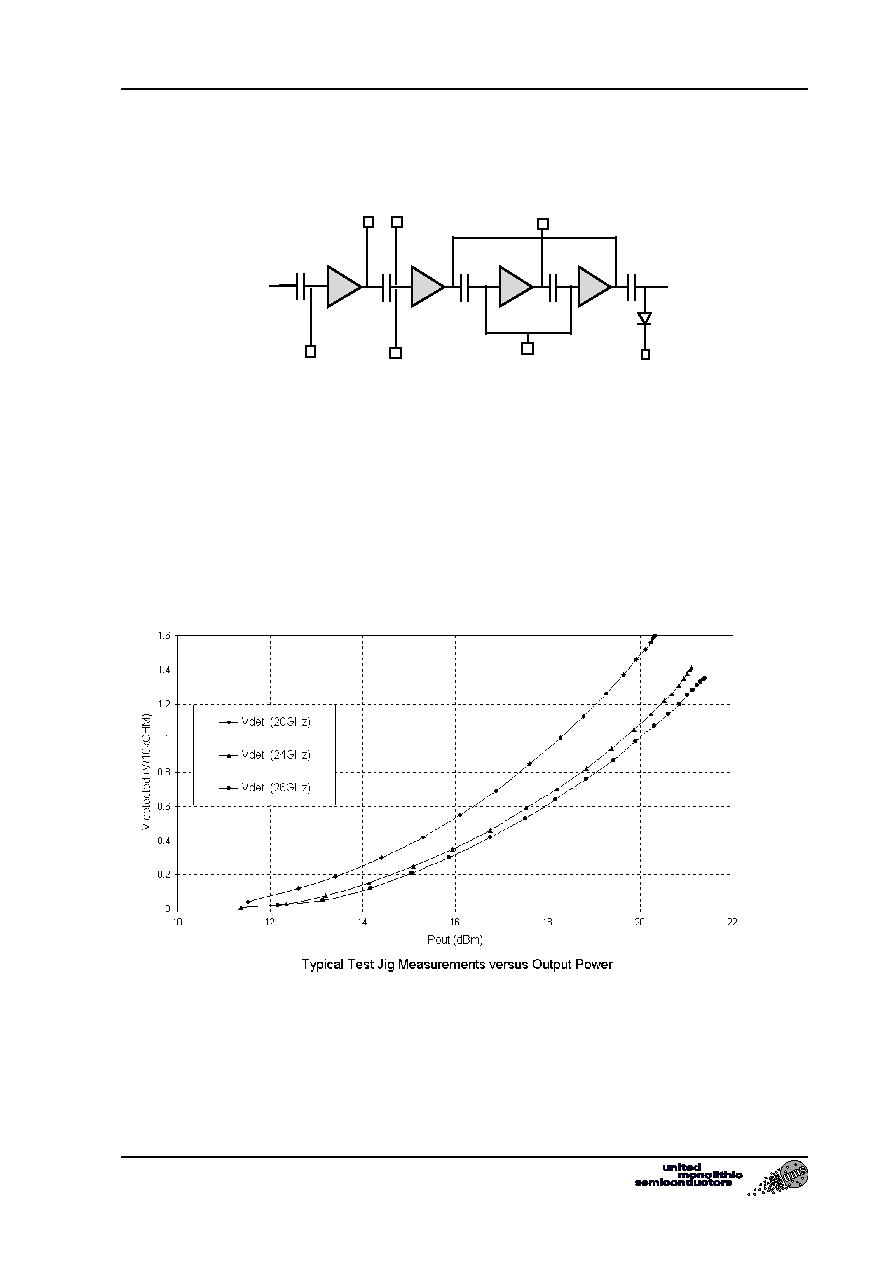
Typical Bias Tuning
The circuit schematic is given below :
IN
OUT
Vd 2,3,4
Vg 3,4
Vg 2
Vg1
Vd1
Vg 2
Vd 2,3,4
Vdet
For medium power operation, the four drain biases are connected altogether. In a same way, all the
gate biases are connected together at the same power supply, tuned to drive a small signal operating
current of 300mA. A separate access to the gate voltages of the two first stages ( Vg1,2 ) is provided in
order to be able to tune the first stages for the application, as a lower noise amplifier or a multiplier.
An additional pad is provided for monitoring the output power, using the Build In Test. This access,
when connected to an external resistor of 10 kOhm ( typical value ) provides a DC voltage which
follows the output power level.
Note : In order to minimize the chip to chip performance spread, it is recommended to bias the chip at
fixed drain current Id rather than at fixed Vg voltage.
In addition, to prevent unwanted self-biasing of the gates under gain compression, it is
preferrable to minimize as much as possible the source resistance of the Vg power supply.