CHA4094
Ref. : DSCHA40949349 ≠ 15 Dec. 99
1/4
Specifications subject to change without notice
United Monolithic Semiconductors S.A.S.
Route DÈpartementale 128 - B.P.46 - 91401 Orsay Cedex France
Tel. : +33 (0)1 69 33 03 08 - Fax : +33 (0)1 69 33 03 09
36-40GHz High Power Amplifier
GaAs Monolithic Microwave IC
Description
The CHA4094 is a high gain broadband three-
stage balanced monolithic power amplifier. It is
designed for a wide range of applications, from
military to commercial communication systems.
The circuit is manufactured with a PM-HEMT
process, 0.25µm gate length, via holes through
the substrate, air bridges and electron beam
gate lithography.
It is available in chip form.
Main Features
Broadband performances
22 dBm output power ( 1dB gain comp. )
9 dB
±
1 dB gain
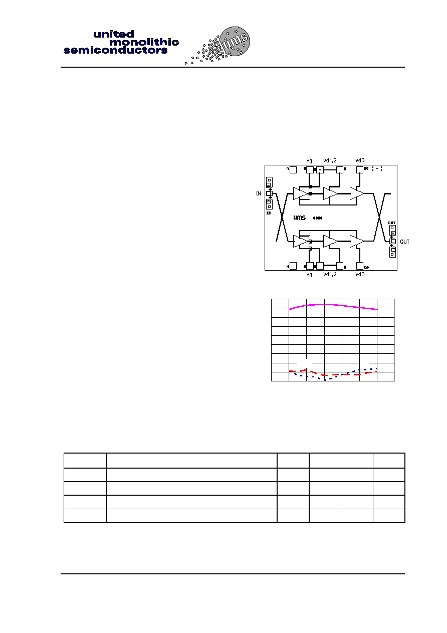
Chip size : 1.65 X 2.05 X 0.10 mm
Typical on wafer measurements :
-30
-25
-20
-15
-10
-5
0
5
10
15
28
30
32
34
36
38
40
42
Frequency (GHz)
(dB)
Gain
IN
OUT
Main Characteristics
Tamb. = 25∞C
Symbol
Parameter
Min
Typ
Max
Unit
Fop
Operating frequency range
36
40
GHz
G
Small signal gain
7
9
dB
P1dB
Output power at 1dB gain compression
22
dBm
Id
Bias current
750
920
mA
ESD Protection : Electrostatic discharge sensitive device. Observe handling precautions !
CHA4094
36-40GHz High Power Amplifier
Ref. : DSCHA40949349 ≠ 15 Dec. 99
2/4
Specifications subject to change without notice
Route DÈpartementale 128 , B.P.46 - 91401 ORSAY Cedex - FRANCE
Tel.: +33 (0)1 69 33 03 08 - Fax : +33 (0)1 69 33 03 09
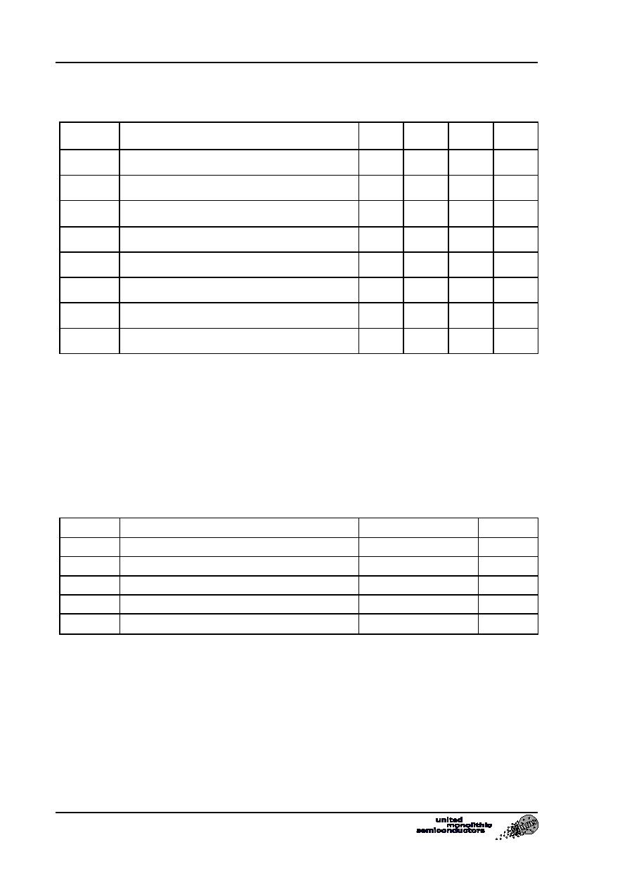
Electrical Characteristics for Broadband Operation
Tamb = +25∞C, Vd1,2,3 = 3.5Volts
Symbol
Parameter
Min
Typ
Max
Unit
Fop
Operating frequency range (1)
36
40
GHz
G
Small signal gain (1) (2)
7
9
dB
G
Small signal gain flatness (1) (2)
±
1
dB
Is
Reverse isolation (1)
30
dB
P1db
Pulsed Output power at 1dB gain compression (1)
22
dBm
VSWRin
Input VSWR (1)
2.0:1
VSWRout Output VSWR (1)
2.0:1
Id
Bias current (3)
750
920
mA
(1) These values are representative of on-wafer measurements that are made without bonding
wires at the RF ports. In the case of a jig or a module CW mode operation, the typical output
power may be around 2dB less.
(2) Vd1, 2, 3 = 2Volts
(3) Depends on Biasing point, see application note for recommended biasing point
Absolute Maximum Ratings
Tamb. = 25∞C (1)
Symbol
Parameter
Values
Unit
Vd
Drain bias voltage
4
V
Id
Drain bias current
1200
mA
Vg
Gate bias voltage
-2 to +0.4
V
Ta
Operating temperature range
-40 to +85
∞C
Tstg
Storage temperature range
-55 to +155
∞C
(1)
Operation of this device above anyone of these parameters may cause permanent damage.
36-40GHz High Power Amplifier
CHA4094
Ref. : DSCHA40949349 ≠ 15 Dec. 99
3/4
Specifications subject to change without notice
Route DÈpartementale 128 , B.P.46 - 91401 ORSAY Cedex - FRANCE
Tel.: +33 (0)1 69 33 03 08 - Fax : +33 (0)1 69 33 03 09
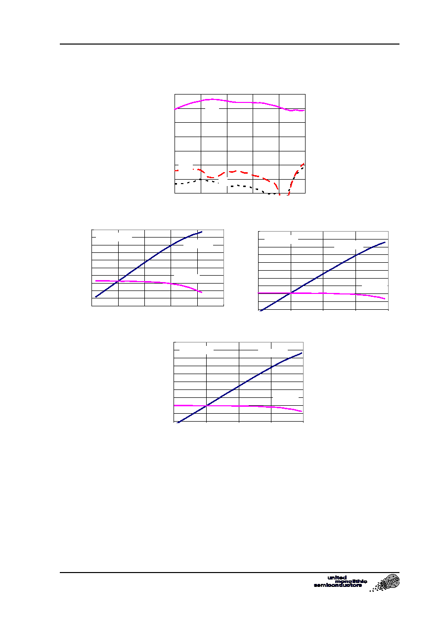
Typical On Jig Measurements
Bias Conditions : Tamb = +25∞C, Vd = 3.5Volt, Vg = -0.2Volt.
-20
-15
-10
-5
0
5
10
15
30
32
34
36
38
40
Frequency (GHz)
(d
B
)
Gain
OUT
IN
5
7
9
11
13
15
17
19
21
23
25
-5
0
5
10
15
20
Input power (dBm)
Freq= 36 GHz
Gain (dB)
Pout (dBm)
5
7
9
11
13
15
17
19
21
23
25
-5
0
5
10
15
Input power (dBm)
Freq= 38GHz
Gain (dB)
Pout (dBm)
5
7
9
11
13
15
17
19
21
23
25
-5
0
5
10
15
Input power (dBm)
Freq= 40GHz
Pout (dBm)
Gain (dB)
Application note
The given DC Bias condition in table or curves are for class A biasing point. This amplifier could be
used in class AB.
For this the Gate voltage must be adjusted for a total drain supply current of typically 500mA.
The loss in linear gain is around 0.4dB, but the output power at 1dB compression point is higher,
between 0.5 and 1dBm more.
This biasing point shows a main advantage in regard of thermal aspect. Indeed the junction
temperature in transistor decreases approximatively of 10∞C for 20% reduction in drain current.
CHA4094
36-40GHz High Power Amplifier
Ref. : DSCHA40949349 ≠ 15 Dec. 99
4/4
Specifications subject to change without notice
Route DÈpartementale 128 , B.P.46 - 91401 ORSAY Cedex - FRANCE
Tel.: +33 (0)1 69 33 03 08 - Fax : +33 (0)1 69 33 03 09
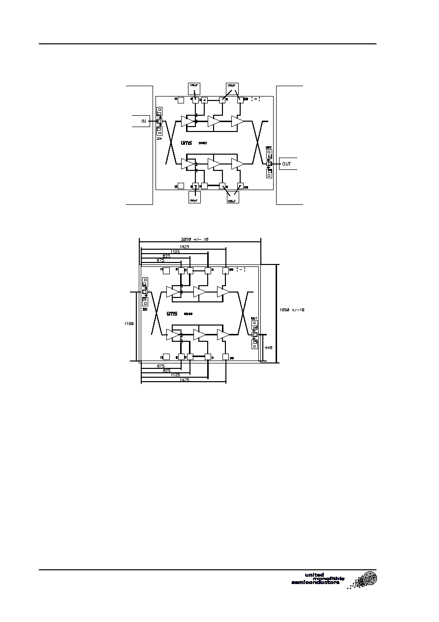
Chip Assembly and Mechanical Data
Note : Supply feed should be capacitively bypassed.
Bonding pad positions.
( Chip thickness : 100µm. All dimensions are in micrometers )
Ordering Information
Chip form
:
CHA4094-99F/00
Information furnished is believed to be accurate and reliable. However united monolithic semiconductors
S.A.S. assumes no responsability for the consequences of use of such information nor for any infringement of
patents or other rights of third parties which may result from its use. No license is granted by implication or
otherwise under any patent or patent rights of united monolithic semiconductors S.A.S.. Specifications
mentioned in this publication are subject to change without notice. This publication supersedes and replaces all
information previously supplied. United monolithic semiconductors S.A.S. products are not authorised for use
as critical components in life support devices or systems without express written approval from united
monolithic semiconductors S.A.S.