CHM1190
Ref. :DSCHM11909025
1/6
Specifications subject to change without notice
United Monolithic Semiconductors S.A.S.
Route DÈpartementale 128 - B.P.46 - 91401 Orsay Cedex France
Tel. : +33 (0)1 69 33 03 08 - Fax : +33 (0)1 69 33 03 09
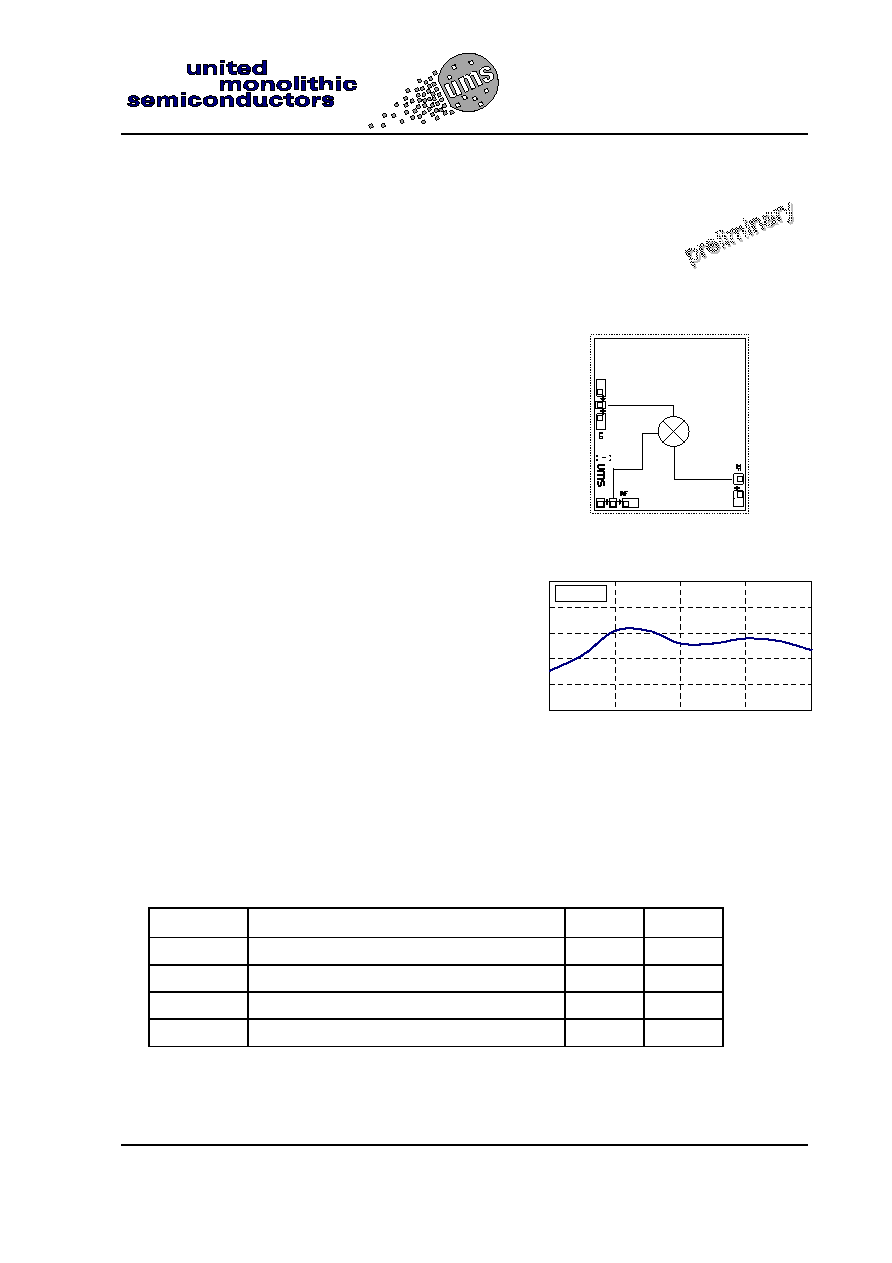
K Band Mixer
GaAs Monolithic Microwave IC
Description
The CHM1190 is a balanced Schottky
diode mixer based on a six quarter wave
ring structure. It could be use in receiver or
transmitter part.
This circuit is manufactured with the BES-
MMIC process: 1 µm Schottky diode
device, air bridges, via holes through the
substrate, stepper lithography.
An electrically identical chip with a mirror
drawing versus de LO side is available
under the part number CHM1191. These
two MMICs could be helpful in a TX, RX
architecture module.
It is available in chip form.
Main Features
22-24 GHz LO frequency range
IF from 1 to 3 GHz
Low conversion loss up & down
High LO/RF isolation
Low LO input power
Small chip size: 1.73 x 1.53 x 0.10 mm
LO
RF
IF
-12
-10
-8
-6
-4
-2
21
22
23
24
25
LO Frequency (GHz)
Conver
si
on gai
n
(
d
B)
IF=2GHz
Typical conversion characteristic
(measurement in test fixture)
Main Characteristics
Tamb. = 25∞C
Symbol
Parameter
Typ
Unit
F_LO,
LO frequency range
22-24
GHz
F_IF
IF frequency range
1 - 3
GHz
Lc
Conversion loss @ P-LO = 7dBm
7
dB
I_LO/RF
LO/RF isolation
30
dBc
ESD Protection : Electrostatic discharge sensitive device. Observe handling precautions !
CHM1190
K band Mixer
Ref. : DSCHM11909025
2/6
Specifications subject to change without notice
Route DÈpartementale 128 , B.P.46 - 91401 ORSAY Cedex - FRANCE
Tel.: +33 (0)1 69 33 03 08 - Fax : +33 (0)1 69 33 03 09
Electrical Characteristics
Tamb. = 25∞C
Symbol
Parameter
Min
Typ
Max
Unit
F_LO
LO frequency range
22
24
GHz
F_IF
IF frequency range
1
3
GHz
Lc
Conversion loss @ P-LO = 7dBm (1)
7
dB
P_LO
LO input power
5
7
9
dBm
P-1dB
Input 1dB compression
7
dBm
VSWR_LO
LO port VSWR (50
) (2)
2.5:1
VSWR_RF
RF port VSWR (50
) (2)
2.5:1
VSWR_IF
RF port VSWR (50
) (2)
2.5:1
I_LO/RF
LO/RF isolation
30
dBc
(1) On wafer measurements.
(2) Depends on the wire bonding conditions and on the external matching network.
Absolute Maximum Ratings (1)
Tamb = +25∞C
Symbol
Parameter
Values
Unit
P_LO
Maximum peak input power overdrive at LO port (2)
10
dBm
P_RF
Maximum peak input power overdrive at RF port (2)
10
dBm
P_IF
Maximum peak input power overdrive at IF port (2)
10
dBm
Top
Operating temperature range
-40 to +85
∞C
Tstg
Storage temperature range
-55 to +125
∞C
(1) Operation of this device above anyone of these parameters may cause permanent damage.
(2) Duration < 1s
K Band Mixer
CHM1190
Ref. : DSCHM11909025
3/6
Specifications subject to change without notice
Route DÈpartementale 128 , B.P.46 - 91401 ORSAY Cedex - FRANCE
Tel.: +33 (0)1 69 33 03 08 - Fax : +33 (0)1 69 33 03 09
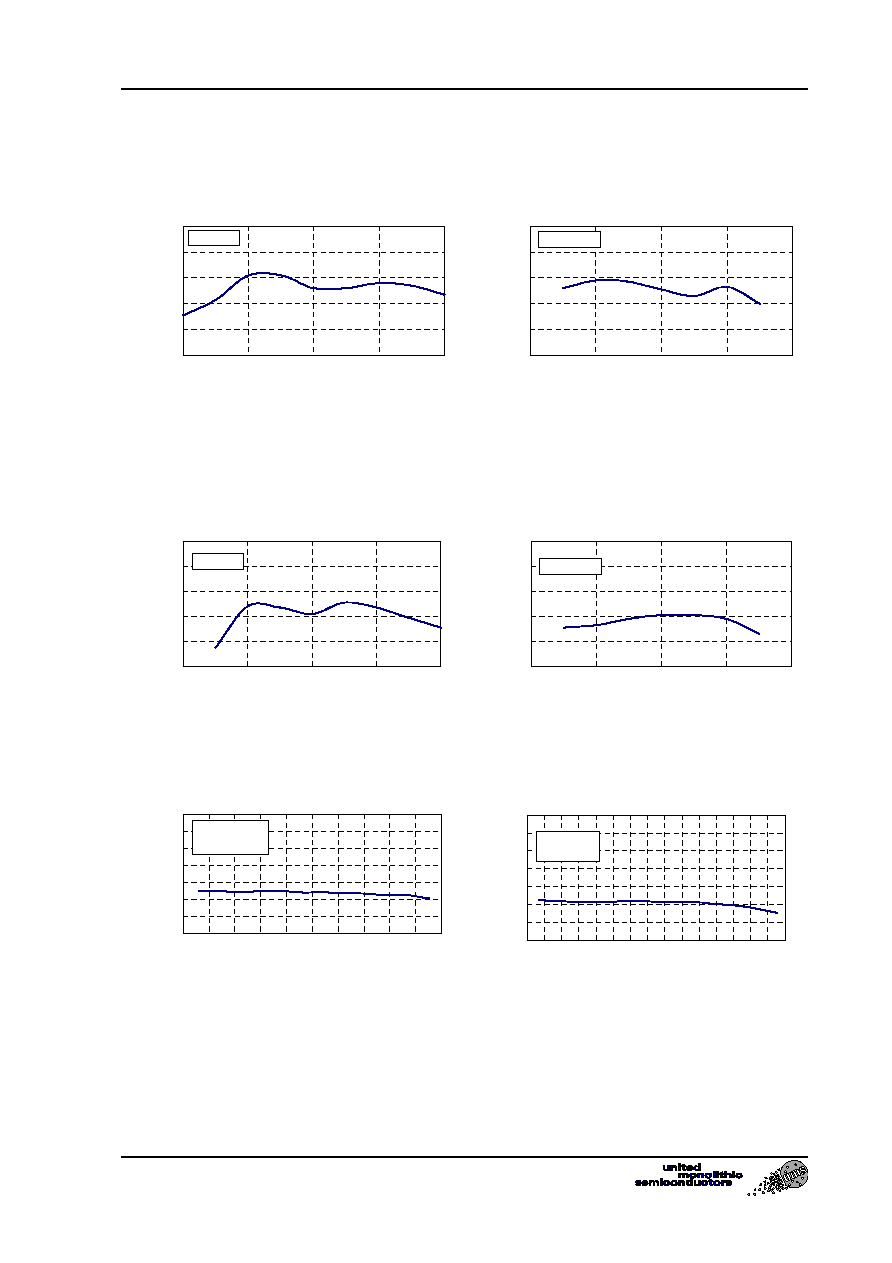
Typical test fixture measurements
Tamb. = 25∞C
A) Down- converter
-12
-10
-8
-6
-4
-2
21
22
23
24
25
LO Frequency (GHz)
Conver
si
on gai
n (
d
B)
IF=2GHz
-12
-10
-8
-6
-4
-2
0
1
2
3
4
IF Frequency (GHz)
Conver
si
on gai
n (
d
B)
LO=23GHz
Conversion gain versus LO frequency Conversion gain versus IF frequency
LO Input power= 9dBm (1)
LO Input power= 9dBm (1)
B) Up- converter
-12
-10
-8
-6
-4
-2
21
22
23
24
25
LO Frequency (GHz)
Conver
si
on gai
n (
d
B)
IF=2GHz
-12
-10
-8
-6
-4
-2
0
1
2
3
4
IF Frequency (GHz)
Conver
si
on gai
n (
d
B)
LO=23GHz
Conversion gain versus LO frequency Conversion gain versus IF frequency
LO Input power= 9dBm (1)
LO Input power= 9dBm (1)
-12
-10
-8
-6
-4
-2
0
2
0
1
2
3
4
5
6
7
8
9
10
RF Input power (dBm)
Conver
si
on gai
n (
d
B)
IF=2GHz
LO=23GHz
-12
-10
-8
-6
-4
-2
0
2
-5 -4 -3 -2 -1 0
1
2
3
4
5
6
7
8
9 10
IF Input power (dBm)
Conver
si
on gai
n (
d
B)
IF=2GHz
LO=23GHz
Input compression point versus RF power
Input compression point versus IF power
LO Input power= 9dBm (1)
LO Input power= 9dBm (1)

CHM1190
K band Mixer
Ref. : DSCHM11909025
4/6
Specifications subject to change without notice
Route DÈpartementale 128 , B.P.46 - 91401 ORSAY Cedex - FRANCE
Tel.: +33 (0)1 69 33 03 08 - Fax : +33 (0)1 69 33 03 09
-25
-20
-15
-10
-5
0
21
22
23
24
25
LO frequency (GHz)
R
e
tu
rn
lo
s
s
(d
B
)
-25
-20
-15
-10
-5
0
22
23
24
25
26
RF frequency (GHz)
R
e
tu
rn
lo
s
s
(d
B
)
LO=23GHz
LO Return loss (1)
RF Return loss (1)
LO input power = 9dBm
LO input power = 9dBm
-25
-20
-15
-10
-5
0
0
1
2
3
4
IF frequency (GHz)
R
e
tu
rn
lo
s
s
(d
B
)
OL=23GHz
IF Return loss
LO input power = 9dBm
(1)
This measurement is made with an external matching network. See application note for
further information.
K Band Mixer
CHM1190
Ref. : DSCHM11909025
5/6
Specifications subject to change without notice
Route DÈpartementale 128 , B.P.46 - 91401 ORSAY Cedex - FRANCE
Tel.: +33 (0)1 69 33 03 08 - Fax : +33 (0)1 69 33 03 09
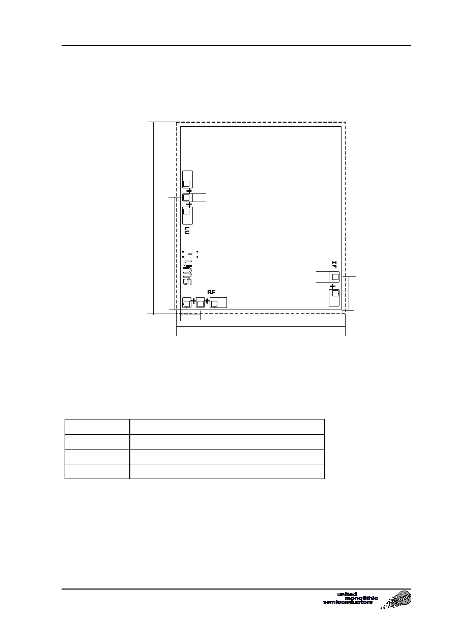
Chip Mechanical Data
(dimensions are in µm)
300
1730 +/- 35
1020
180
1530+/-35
70
96
Chip size (including saw streets) : 1730 x 1530
±
35µm
Thickness: 100µm
±
10µm
Pin
Description
LO
LO input signal
RF
RF input or output signal
IF
IF input or output signal
An electrically identical chip with a mirror drawing versus de LO side is available under the
part number CHM1191.