 | –≠–ª–µ–∫—Ç—Ä–æ–Ω–Ω—ã–π –∫–æ–º–ø–æ–Ω–µ–Ω—Ç: CHP2085 | –°–∫–∞—á–∞—Ç—å:  PDF PDF  ZIP ZIP |

CHP2085
Ref. : DSCHP20850046 - 15-feb.-00
1/6
Specifications subject to change without notice
United Monolithic Semiconductors S.A.S.
Route DÈpartementale 128 - B.P.46 - 91401 Orsay Cedex France
Tel. : +33 (0)1 69 33 03 08 - Fax : +33 (0)1 69 33 03 09
S-band Phase Shifter / Switch
GaAs Monolithic Microwave IC
Description
The CHP2085 is a S-band monolithic
5 bits phase shifter / switch.
The circuit is manufactured with a
standard MESFET process : via holes
through the substrate, air bridges and
electron beam gate lithography.
It is supplied in chip form.
Main Features
Frequency range : 2.7 to 3.4GHz
11.25∞ phase quantization
27dB switch isolation
Chip size : 4,14 x 2,16 x 0,1mm
12
11
10
13
14
1
9
8
7
6
5
4
3
2
Switch
22,5∞ bit
180∞ bit
90∞ bit
45
∞ bit
11,25∞ bit
Pin Out
1- RFout2
8- B4
2- P2
9- H4
3- P1
10- BH1
4- H8
11- GND
5- B8
12- B9
6- B2
13- RFin
7- H9
14- RFout1
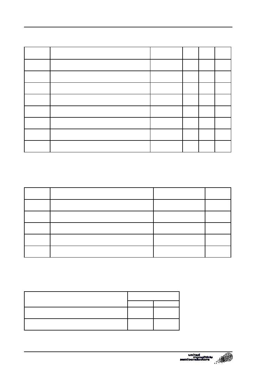
Main Characteristics
Tamb = +25∞C
Symbol
Parameter
Min
Max
Unit
Fop
Operating frequency range
2.7
3.4
GHz
PHIpp
Phase shift precision peak to peak error
10
∞
Il
Insertion loss
12
dB
Is
Isolation
27
dB
ESD Protections : Electrostatic discharge sensitive device observe handling precautions !
CHP2085
S-band Phase Shifter / Switch
Ref. : DSCHP20850046 - 15-feb.-
00DSCHP20850046 - 15-feb.-00
2/6
Specifications subject to change without notice
Route DÈpartementale 128 , B.P.46 - 91401 ORSAY Cedex - FRANCE
Tel.: +33 (0)1 69 33 03 08 - Fax : +33 (0)1 69 33 03 09
Electrical Characteristics
Tamb = +25∞C
Symbol
Parameter
Test
Conditions
Min
Max
Unit
Fop
Operating frequency range
2.7
3.4
GHz
PHIpp
Phase shift precision peak to peak error
(1)
10
∞
Il
Insertion loss
(1)
12
dB
Is
Isolation
(1)
27
dB
VSWRin
Input VSWR
(1)
2:1
VSWRout Ouput VSWR
(1)
2:1
Pin1dB
Pulsed Input power at 1dB increase loss
(2)
23
dBm
Ips
Phase shifter current
(1)
5
mA
(1) Pin
0dBm, Low level control voltage = -4V, High level control voltage = 0V,
Vgi consistent with the Phase Schifter Control Interface table.
(2) These values are representative for pulsed on-wafer measurements
Absolute Maximum Ratings
(1)
Tamb = +25∞C
Symbol
Parameter
Values
Unit
Vgi
Phase shifter control voltage
-8.0
V
Vpi
Switch control voltage
-8.0
V
Pin
Maximum peak input power overdrive (2)
+25
dBm
Top
Operating temperature range
-40 to +85
∞C
Tstg
Storage temperature range
-55 to +125
∞C
(1) Operation of this device above anyone of these paramaters may cause permanent damage.
(2) Duration < 1s.
(1) Pin
0dBm
Switch Control Signal Interface
Switch command
Bond pads
P1
P2
Rfin to RFout2
Low level High level
Rfin to RFout1
High level Low level
S-band Phase Shifter / Switch
CHP2085
Ref. : DSCHP20850046 - 15-feb.-00
3/6
Specifications subject to change without notice
Route DÈpartementale 128 , B.P.46 - 91401 ORSAY Cedex - FRANCE
Tel.: +33 (0)1 69 33 03 08 - Fax : +33 (0)1 69 33 03 09
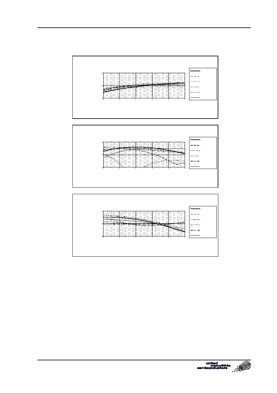
Typical Wafer [S] Parameters
RFin to RFout2 path
IN SERT IO N LO SS
-1 0 ,0 0
-8 ,0 0
-6 ,0 0
2 , 5
2 , 7
2 , 9
3 ,1
3 ,3
3 , 5
FREQ (GH z)
(d
B
)
rÈf
1 1 . 2 5 ∞
2 2 . 5 ∞
4 5 ∞
9 0 ∞
1 8 0 ∞
RET U RN LO SS (IN )
-3 0 ,0 0
-2 0 ,0 0
-1 0 ,0 0
2 , 5
2 , 7
2 , 9
3 ,1
3 ,3
3 , 5
FREQ (GH z)
(d
B
)
rÈf
1 1 . 2 5 ∞
2 2 . 5 ∞
4 5 ∞
9 0 ∞
1 8 0 ∞
RET U RN LO SS (O U T )
-3 0 , 0 0
-2 0 , 0 0
-1 0 , 0 0
2 , 5
2 ,7
2 , 9
3 ,1
3 , 3
3 , 5
FREQ (GH z)
(d
B
)
rÈf
1 1 . 2 5 ∞
2 2 . 5 ∞
4 5 ∞
9 0 ∞
1 8 0 ∞
CHP2085
S-band Phase Shifter / Switch
Ref. : DSCHP20850046 - 15-feb.-
00DSCHP20850046 - 15-feb.-00
4/6
Specifications subject to change without notice
Route DÈpartementale 128 , B.P.46 - 91401 ORSAY Cedex - FRANCE
Tel.: +33 (0)1 69 33 03 08 - Fax : +33 (0)1 69 33 03 09
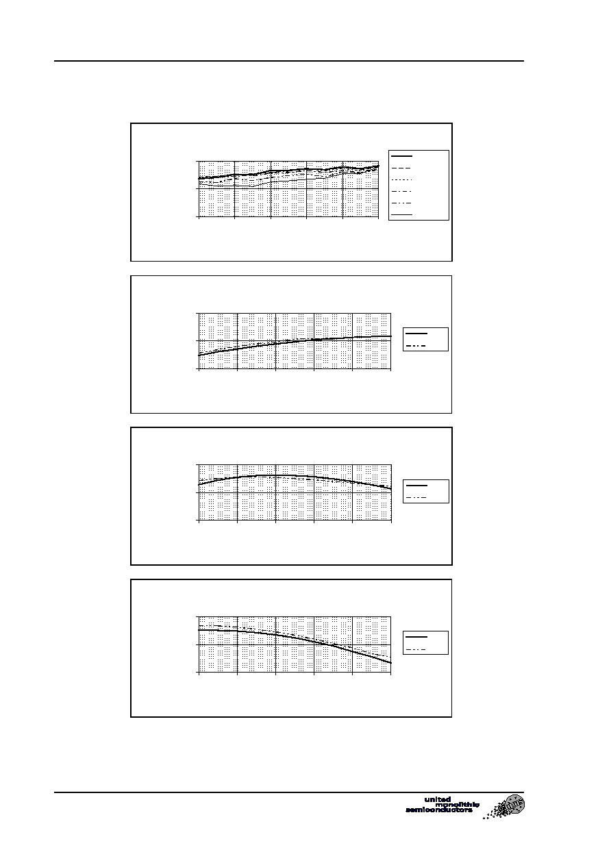
Typical Wafer [S] Parameters
RFin to RFout1 path
ISO LA T IO N
-4 0 , 0 0
-3 5 , 0 0
-3 0 , 0 0
2 , 5
2 ,7
2 , 9
3 ,1
3 , 3
3 , 5
FREQ (GH z)
(d
B
)
rÈf
1 1 . 2 5 ∞
2 2 . 5 ∞
4 5 ∞
9 0 ∞
1 8 0 ∞
IN SERT IO N LO SS
-1 0 ,0 0
-8 ,0 0
-6 ,0 0
2 , 5
2 , 7
2 ,9
3 , 1
3 , 3
3 , 5
FREQ (GH z)
(d
B
)
rÈf
9 0 ∞
RET U RN LO SS (IN )
-3 0 , 0 0
-2 0 , 0 0
-1 0 , 0 0
2 , 5
2 , 7
2 , 9
3 ,1
3 ,3
3 , 5
FREQ (GH z)
(d
B
)
rÈf
9 0 ∞
RET U RN LO SS (OU T )
-3 0 ,0 0
-2 0 ,0 0
-1 0 ,0 0
2 , 5
2 , 7
2 ,9
3 , 1
3 , 3
3 , 5
FREQ (GH z)
(d
B
)
rÈf
9 0 ∞
S-band Phase Shifter / Switch
CHP2085
Ref. : DSCHP20850046 - 15-feb.-00
5/6
Specifications subject to change without notice
Route DÈpartementale 128 , B.P.46 - 91401 ORSAY Cedex - FRANCE
Tel.: +33 (0)1 69 33 03 08 - Fax : +33 (0)1 69 33 03 09
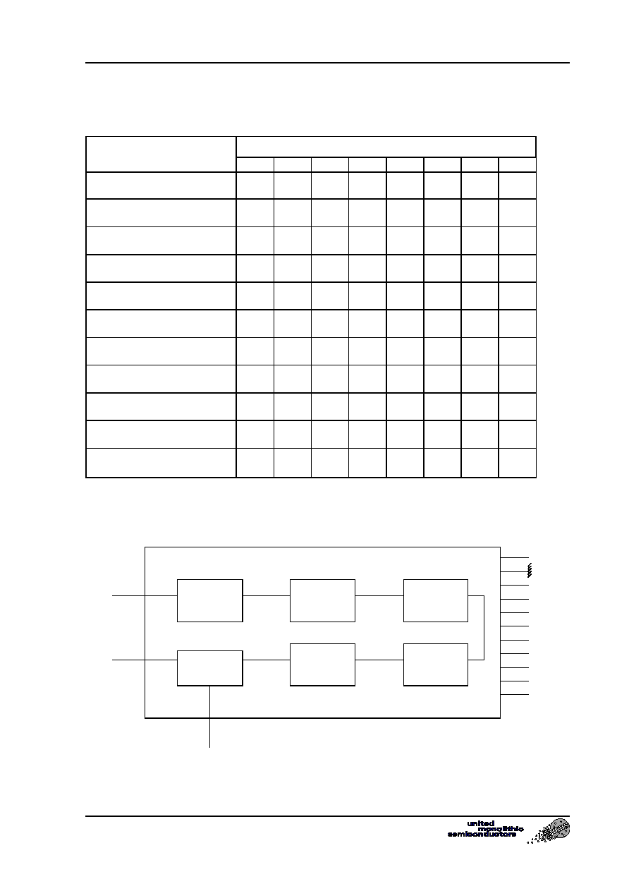
Phase Shifter Control Interface
The 5 bits phase shifter command is actuated by the 8 voltage control pads
State = 1 for Vgi = 0V (high level), State = 0 for Vgi = -5.5V (low level)
Nominal phase state
Bond pads (1)
∞
H8
B8
H9
B9
H4
B4
B2
BH1
0
(0)
1
0
1
0
1
0
0
0
11.25 (
/16)
1
0
1
0
1
0
0
1
22.50 (
/8)
1
0
1
0
1
0
1
0
33.75 (
/8 +
/16)
1
0
1
0
1
0
1
1
45
(
/4)
1
0
1
0
0
1
0
0
56.25 (
/4 +
/16)
1
0
1
0
0
1
0
1
67.50 (
/4 +
/8)
1
0
1
0
0
1
1
0
78.75 (
/4 +
/8 +
/16)
1
0
1
0
0
1
1
1
90
(
/2)
1
0
0
1
1
0
0
0
180
(
)
0
1
1
0
1
0
0
0
348.75 (
+
/2 +
/4 +
/8 +
/16)
0
1
0
1
0
1
1
1
(1)
Terminology :
B = Low pass, H = High pass, BH = Low/High pass
1 = 11∞5, 2 = 22.5∞, 4 = 45∞, 9 = 90∞, 8 = 180∞
Simplified Schematic
RFin
RFout1
RFout2
90∞ bit
45∞ bit
11,25∞ bit
22,5∞ bit
180∞ bit
Switch
B9
BH1
H4
B4
H9
B2
B8
H8
P1
P2