 | –≠–Ľ–Ķ–ļ—ā—Ä–ĺ–Ĺ–Ĺ—č–Ļ –ļ–ĺ–ľ–Ņ–ĺ–Ĺ–Ķ–Ĺ—ā: CHR0100A | –°–ļ–į—á–į—ā—Ć:  PDF PDF  ZIP ZIP |
CHR0100a
Ref. : DSCHR01000161 -9-Jun-00
1/6
Specifications subject to change without notice
United Monolithic Semiconductors S.A.S.
Route Dťpartementale 128 - B.P.46 - 91401 Orsay Cedex France
Tel. : +33 (0)1 69 33 03 08 - Fax : +33 (0)1 69 33 03 09
5.8GHz I/Q Mixer
GaAs Monolithic Microwave IC
Description
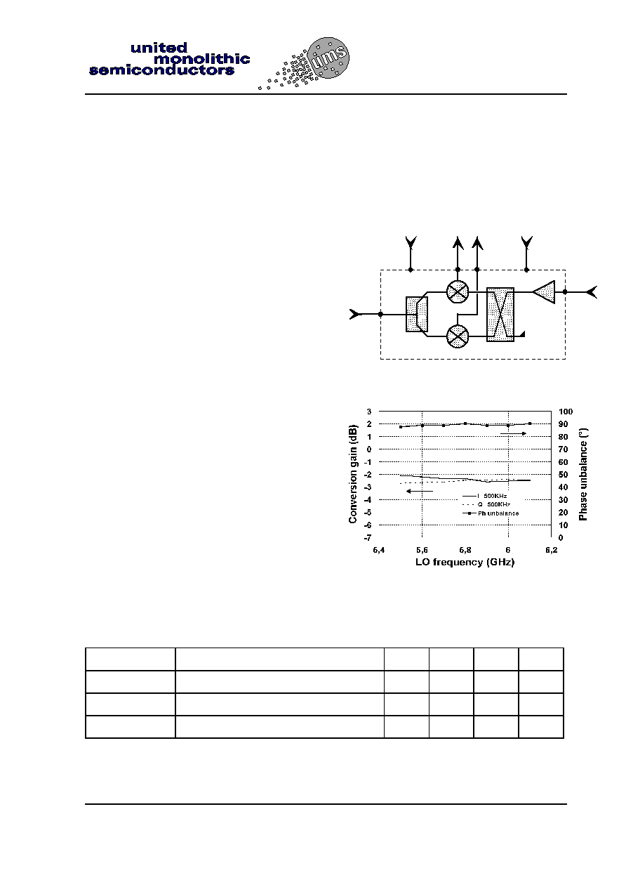
The CHR0100a is a single chip MMIC
including an I/Q mixer and a RF gain block
that minimises the overall conversion loss of
the receiver and provides the RF signal to
the mixer through a power divider.
The circuit is manufactured with the P-
HEMT process : 0.25Ķm gate length, via
holes through the substrate, air bridges
and electron beam gate lithography.
It is supplied in chip form or in ceramic
leadless chip carrier.
Main Features
5.8GHz centre frequency
DC-50MHz IF bandwidth
Low noise figure
Low I/Q phase & amplitude unbalance
Chip size : 1.77 x 1.37 x 0.10 mm
Vd
Vg
RF
LO
I
Q
Block diagram
Conversion gain (RF to I; RF to Q)
and phase unbalance
Main Characteristics
Tamb = +25įC
Symbol
Parameter
Min.
Typ.
Max.
Unit
Fop
Operating frequency range
5.725
5.8
5.875
GHz
Cg
Conversion gain (RF to I; RF to Q)
-4
-2.5
dB
Plo
LO input power
6
dBm
ESD Protections : Electrostatic discharge sensitive device observe handling precaution !
CHR0100a
5.8GHz Image rejection mixer
Ref. : DSCHR01000161 -9-Jun-00
2/6
Specifications subject to change without notice
Route Dťpartementale 128 , B.P.46 - 91401 ORSAY Cedex - FRANCE
Tel.: +33 (0)1 69 33 03 08 - Fax : +33 (0)1 69 33 03 09
Electrical Characteristics
Tamb = +25įC
Symbol
Parameter
Test
conditions
Min.
Typ.
Max.
Unit
Fop
Operating frequency range
5.725
5.8
5.875
GHz
BWif
IF frequency band
DC
50
MHz
Cg
Conversion gain, RF to I or RF to Q
(1)
-4
-2.5
dB
NF
Noise figure (DSB), RF to I or RF to Q
IF=10MHz
5
dB
Pif_1dB
I or Q IF output power at 1dB
compression gain
-5
dBm
Plo
LO input power
5
8
dBm
I/Q phase unbalance
10
15
į
Cg
I/Q amplitude unbalance
0.5
1.0
dB
Vd
Positive bias voltage
4
V
Id
Bias current
15
25
mA
(1) Conversion gain will be 3dB higher after I/Q combination.
Absolute Maximum Ratings (1)
Tamb = +25įC
Symbol
Parameter
Values
Unit
Vd
Positive supply voltage
6
V
Vg
Negative supply voltage
-2 to 0
V
Pin
Maximum peak input power overdrive (2)
10
dBm
Top
Operating temperature range
-50 to 70
įC
Tstg
Storage temperature range
-55 to 155
įC
(1) Operation of this device above anyone of these parameters may cause permanent damage
(2) Duration < 1s.

5.8GHz Image Rejection Mixer
CHR0100a
Ref. : DSCHR01000161 -9-Jun-00
3/6
Specifications subject to change without notice
Route Dťpartementale 128 , B.P.46 - 91401 ORSAY Cedex - FRANCE
Tel.: +33 (0)1 69 33 03 08 - Fax : +33 (0)1 69 33 03 09
Chip Pad Allocation
CHR0100a
Q
Q
I
LO
RF
VgQ
VgQ
VgI
Vd
Input And Output Pin References
Pin
Description
RF
RF signal input
LO
LO signal input
VgI
I mixer negative supply voltage
VgQ
Q mixer negative supply voltage
Vd
Positive supply voltage
I
First IF output
Q
Second IF output (in quadrature)
Connection of only one of the two VgQ and Q pads is necessary
VgI, VgQ only necessary for low LO power

CHR0100a
5.8GHz Image rejection mixer
Ref. : DSCHR01000161 -9-Jun-00
4/6
Specifications subject to change without notice
Route Dťpartementale 128 , B.P.46 - 91401 ORSAY Cedex - FRANCE
Tel.: +33 (0)1 69 33 03 08 - Fax : +33 (0)1 69 33 03 09
Typical Bias Configuration
The typical bias voltage applied to the chip is Vd = 4V.
If the LO power is low (ex: < 5dBm) one can apply a negative voltage (-0.3V) on
Vg to improve and secure the conversion characteristic.
Each Vg and Vd port should have a 10nF decoupling capacitor to the ground.
Connection of only one of the two VgQ and Q pads is necessary
CHR0100a
Q
Q
I
LO
RF
10nF
VgI
10nF
VgQ
10nF
Vd
10nF
VgQ
Chip Mechanical Data
CHR0100a
Chip size 1770
Ī
20 Ķm x 1370
Ī
20 Ķm
Chip thickness 100
Ī
10 Ķm

5.8GHz Image Rejection Mixer
CHR0100a
Ref. : DSCHR01000161 -9-Jun-00
5/6
Specifications subject to change without notice
Route Dťpartementale 128 , B.P.46 - 91401 ORSAY Cedex - FRANCE
Tel.: +33 (0)1 69 33 03 08 - Fax : +33 (0)1 69 33 03 09
General tolerance
Package Pin Allocation (SJ)
Pin
Number
Description
RF
20
RF signal input
LO
11
LO signal input
VgI
7
I mixer negative supply voltage
VgQ
6
Q mixer negative supply voltage
Vd
1
Positive supply voltage
I
4
First IF output
Q
3
Second IF output (in quadrature)
10,12,15,17,
19,21
GROUND
2,5,8,9,13,14,
16,18,22,23,24
Not connected