CHV2240
Ref. :DSCHV22400096 -05-Apr-00
1/8
Specifications subject to change without notice
united monolithic semiconductors S.A.S.
Route DÈpartementale 128 - B.P.46 - 91401 Orsay Cedex France
Tel. : +33 (0)1 69 33 03 08 - Fax : +33 (0)1 69 33 03 09
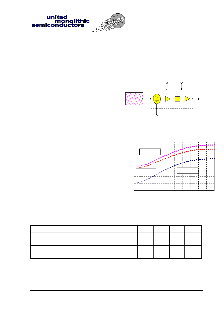
Multifunction : K-band VCO and Q-band Multiplier
GaAs Monolithic Microwave IC
Description
The CHV2240 is a monolithic multifunction
proposed for frequency generation at
38GHz. It integrates a K-band Voltage
Controlled Oscillator, a Q-band frequency
multiplier and buffer amplifiers. For
performance optimisation, an external port
(ERC) allows a passive resonator coupling
to the oscillator (at half output frequency).
This chip has been especially designed to
be coupled to a high Q dielectric resonator.
All the active devices are internally self
biased.
The circuit is manufactured with the P-
HEMT process : 0.25µm gate length, via
holes through the substrate, air bridges
and electron beam gate lithography.
It is available in chip form.
Main Features
n
K-band VCO + Q-band frequency
multiplier
n
External resonator for centre frequency
control and phase noise optimisation
n
High quality oscillator when coupled to
a dielectric resonator
n
On-chip varactor for electronic control
n
Chip size 2.68x1.4 x 0.1 mm
(F_out)
HIGH Q
HIGH Q
HIGH Q
HIGH Q
RESONATOR
RESONATOR
RESONATOR
RESONATOR
F_out/2
x2
RF_out
V_tune
+V
-V
ERC
Multifunction block diagram
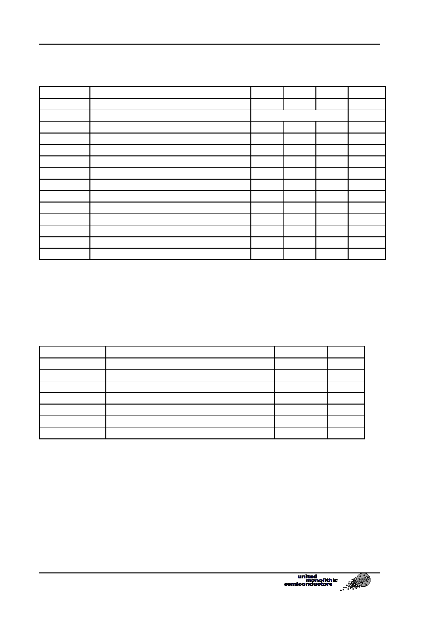
38,19
38,192
38,194
38,196
38,198
38,2
38,202
38,204
0
0,2
0,4
0,6
0,8
1
1,2
1,4
1,6
1,8
2
Vtune (V)
Output frequency
(GHz)
Typical tuning characteristic
Main Characteristics
Tamb = +25∞C
Symbol
Parameter
Min
Typ
Max
Unit
F_out
Output frequency
37.5
38.25
39
GHz
F_t
Frequency tuning range (high Q resonator)
5
MHz
Pn
Oscillator phase noise @ 100kHz (38GHz)
-100
dBc/Hz
Pout
Output power
9
dBm
ESD Protections : Electrostatic discharge sensitive device observe handling precautions !
T=+100∞C
T=-40∞C
T=+25∞C
CHV2240
K-band VCO / Q-band Multiplier
Ref. :DSCHV22400096 -05-Apr-00
2/8
Specifications subject to change without notice
Route DÈpartementale 128 , B.P.46 - 91401 ORSAY Cedex - FRANCE
Tel.: +33 (0)1 69 33 03 08 - Fax : +33 (0)1 69 33 03 09
Electrical Characteristics
Full temperature range, used according to section "Typical assembly and bias configuration"
Symbol
Parameter
Min
Typ
Max
Unit
F_out
Output frequency
37.5
38.25
39
GHz
F_osc
Oscillator frequency (1)
F_out/2
F_stab
Frequency stability (1) , (2)
4
ppm/∞C
Pn
Phase noise @ 100kHz @ 38GHz (2)
-100
dBc/Hz
P_out
Output power
6
9
dBm
F_t
Frequency tuning range (2)
5
MHz
Vt
Voltage tuning range
0-2
V
I_vt
Tuning current
0.5
mA
VSWR_out
VSWR at output port
2:1
+V
Positive supply voltage
4.4
4.5
4.6
V
+I
Positive supply current
120
180
mA
-V
Negative supply voltage
-4.6
-4.5
-4.4
V
-I
Negative supply current
3
10
mA
Top
Operating temperature range
-40
+100
∞C
(1) The centre frequency is given by the external passive resonator
(2) This characteristic is obtained by using an external dielectric resonator (see section
"Proposed External High Q resonator")
Absolute Maximum Ratings (1)
Tamb = +25∞C
Symbol
Parameter
Values
Unit
P_erc
RF input power on ERC port (2)
13
dBm
+V
Positive supply voltage
5
V
-V
Negative supply voltage
-5
V
+I
Positive supply current
200
mA
-I
Negative supply current
10
mA
Top
Operating temperature range
-40 to +100
∞C
Tstg
Storage temperature range
-55 to +155
∞C
(1)
Operation of this device above anyone of these parameters may cause permanent damage.
(2)
Duration < 1s
K-band VCO / Q-band Multiplier
CHV2240
Ref. :DSCHV22400096 -05-Apr-00 dd-Mmm-yy
3/8
Specifications subject to change without notice
Route DÈpartementale 128 , B.P.46 - 91401 ORSAY Cedex - FRANCE
Tel.: +33 (0)1 69 33 03 08 - Fax : +33 (0)1 69 33 03 09
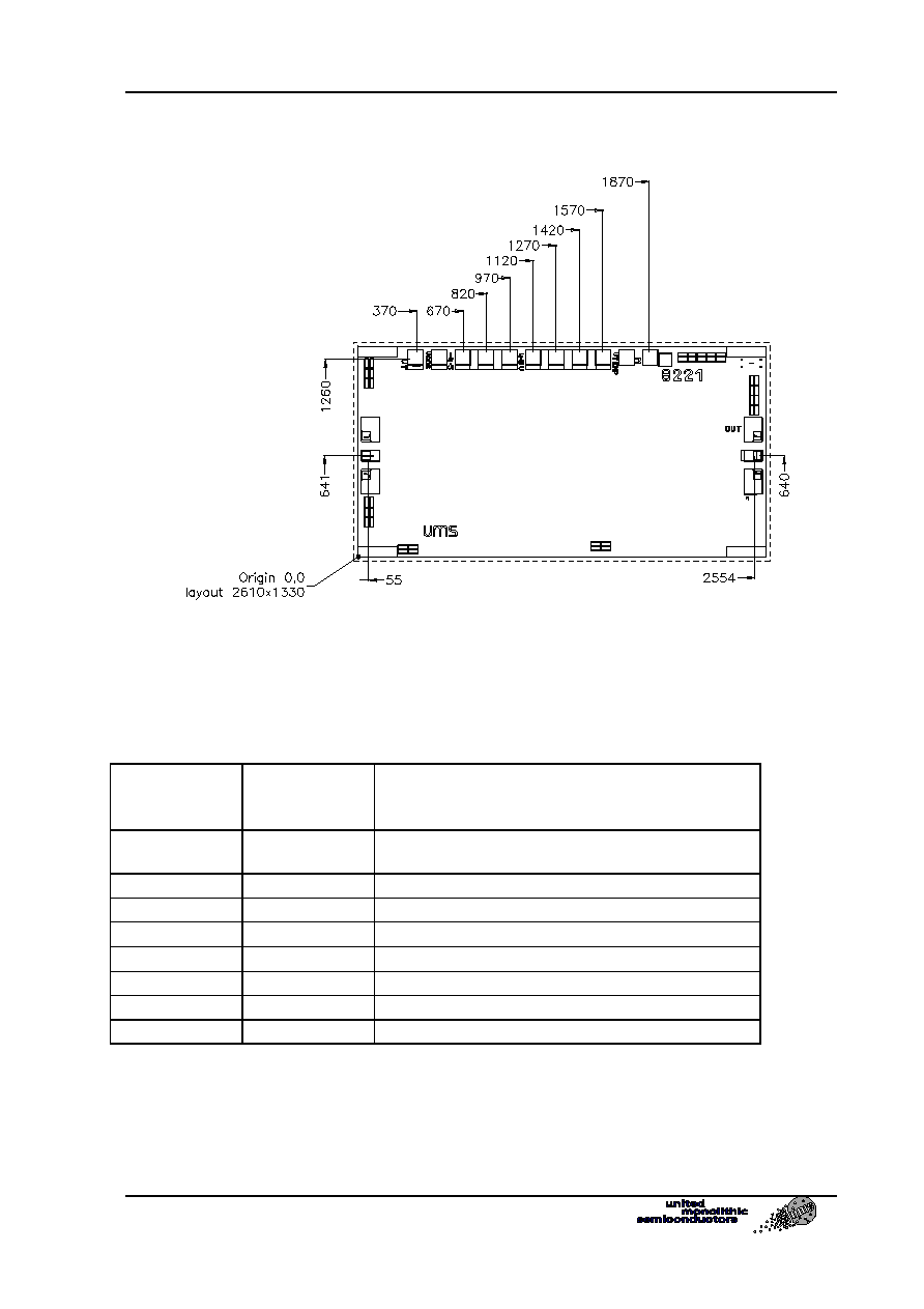
Chip Mechanical Data and Pin References
1
2
3
4
5
6
7
8
9
10
11 12 13 14
15
16
17
Unit = µm
External chip size (layout size + dicing streets) = 2680 x 1400
Chip thickness = 100 +/- 10
HF Pads (2, 16) = 68 x 118
DC/IF Pads = 100 x 100
Pin
number
Pin name
Description
1,3,15,17
Ground : should not be bonded. If required,
please ask for more information.
2
ERC
External Resonator Coupling Port
4
Vt
Tuning voltage
5,13
NC
6,7,8
-V
Negative supply voltage (connected together)
9,10,11,12
+V
Positive supply voltage (connected together)
14
GND
Ground (optional)
16
RF_out
RF output
CHV2240
K-band VCO / Q-band Multiplier
Ref. :DSCHV22400096 -05-Apr-00
4/8
Specifications subject to change without notice
Route DÈpartementale 128 , B.P.46 - 91401 ORSAY Cedex - FRANCE
Tel.: +33 (0)1 69 33 03 08 - Fax : +33 (0)1 69 33 03 09
Typical Assembly and Bias Configuration
1
2
3
4
5
6
7
8
9
10
11 12 13 14
15
16
17
-V
+V
DC/IF lines
>= 120pF
>= 120pF
Vt
L_erc
µ-strip line
L_out
µ-strip line
This drawing shows an example of assembly and bias configuration. All
the transistors are internally self biased.
For the RF pads the equivalent wire bonding inductance (diameter=25µm)
have to be according to the following recommendation.
Port
Equivalent inductance
(nH)
Approximated wire
length (mm)
ERC (2)
L_erc = 0.4
0.5
RF_out (16)
L_out = 0.4
0.5
For a micro-strip configuration a hole in the substrate is recommended for chip
assembly.
K-band VCO / Q-band Multiplier
CHV2240
Ref. :DSCHV22400096 -05-Apr-00 dd-Mmm-yy
5/8
Specifications subject to change without notice
Route DÈpartementale 128 , B.P.46 - 91401 ORSAY Cedex - FRANCE
Tel.: +33 (0)1 69 33 03 08 - Fax : +33 (0)1 69 33 03 09
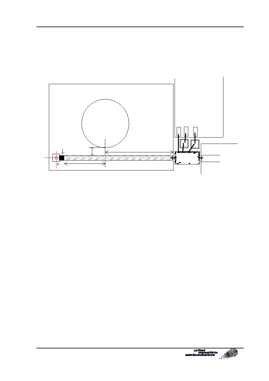
Proposed external high Q resonator
This chip has been especially designed to be coupled to a high Q
dielectric resonator. The resonance is given by a dielectric cylinder coupled to a
50
line. The size of the resonator gives the centre frequency and the space
between the resonator and the line gives the loaded quality factor. The following
drawing shows an example of external configuration.
Dielectric
resonator
Alumina substrate : thickness=250µm
50 Ohm resistance
via hole
3xl
2xl
d
1
2
3
4
5
6
7
8
9
10
11
12
13
14
15
16
17
Additional information
n
Resonator reference example = MURATA /DRD036EC016. As the
exact frequency is given by the resonator size but also by the
environment (cavity size, substrate characteristics, parasitic couplings
...), the final dimensions of the resonator have to be defined according
to the definitive module design. Other kind of resonators can be used
(from TEKELEC or TRANS-TECH). The temperature coefficient has to
be chosen according to the environment.
n
Resonator coupling : d=0.2 to 0.3mm , l=1.5mm (quarter wave).
These values have been used in the test fixture, of course they can be
modified if the environment is different. The distance between the
resonator and the edge of the substrate (close to MMIC) is proposed
to be 3xl=4.5mm (3 quarter waves), theoretically only one is necessary
but in this case the distance between resonator and MMIC is too low
for automatic assembly.
n
50
line width on alumina (heigth=0.25mm) = 0.238mm
n
50
load on alumina : this load has to be as good as possible (low
parasitic inductance).
n
Cavity size (mm) : 18 x 17 x 7