
DBES105a
Ref. : DSDBES1051067 -08-Mar-01
1/4
Specifications subject to change without notice
United Monolithic Semiconductors S.A.S.
Route DÈpartementale 128 - B.P.46 - 91401 Orsay Cedex France
Tel. : +33 (0)1 69 33 03 08 - Fax : +33 (0)1 69 33 03 09
Flip-Chip Dual Diode
GaAs Diode
Description
The DBES105a is a dual Schottky diode based
on a low cost 1µm stepper process including a
bump technology. The parasitic inductances are
reduced and result in a very high operating
frequency.
This flip-chip dual diode has been designed for
high performance mixer applications.
Main Features
High cut-off frequencies : 3THz
High breakdown voltage : < -5V
@ 20µA
Good ideality factor : 1.2
Low parasitic inductances
Low cost technology
Dimensions : 0.53 x 0.23 x 0.1mm
Main Characteristics
Tamb. = 25∞C
Symbol
Parameter
Typ
Unit
Wu
Gate Width
5
µm
Fco
Cut-off frequency
3
THz
n
Ideality factor
1.2
BVak
Anode-cathode break-down voltage
< -5
V
ESD Protection : Electrostatic discharge sensitive device. Observe handling precautions !
DBES105a
Flip-Chip Dual Diode
Ref. : DSDBES1051067 -08-Mar-01
2/4
Specifications subject to change without notice
Route DÈpartementale 128 , B.P.46 - 91401 ORSAY Cedex - FRANCE
Tel.: +33 (0)1 69 33 03 08 - Fax : +33 (0)1 69 33 03 09
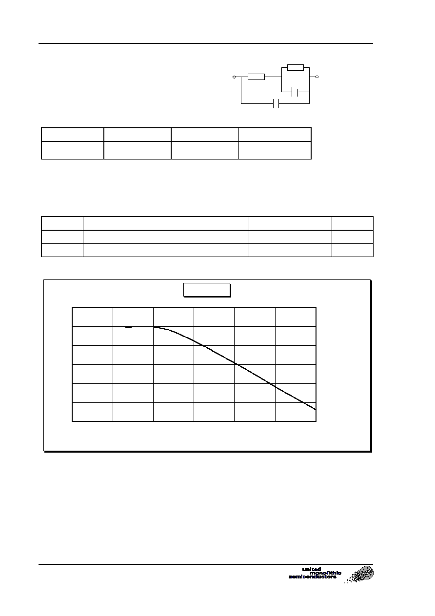
Equivalent Circuit
Rs(
)
Cjo(fF) (0V)
Cpar(fF)
Fco(THz)
4.4
9.5
5.8
2.4
Fco = 1/(2
Rs [Cpar + Cjo])
Rp can be neglected
Absolute Maximum Ratings
(1)
Tamb. = 25∞C
Symbol
Parameter
Typ. values
Unit
Vak
Reverse anode-cathode voltage
-5
V
Iak
Forward anode-cathode current
10
mA
(1) Operation of this device above anyone of these parameters may cause permanent damage.
Imax vs Tamb
0
2
4
6
8
10
12
0
20
40
60
80
100
120
Tam b (∞C)
I m
ax( m
A
)
Rp
Rs
Cj0
Cpar
Flip-Chip Dual Diode
DBES105a
Ref. : DSDBES1051067 -08-Mar-01
3/4
Specifications subject to change without notice
Route DÈpartementale 128 , B.P.46 - 91401 ORSAY Cedex - FRANCE
Tel.: +33 (0)1 69 33 03 08 - Fax : +33 (0)1 69 33 03 09
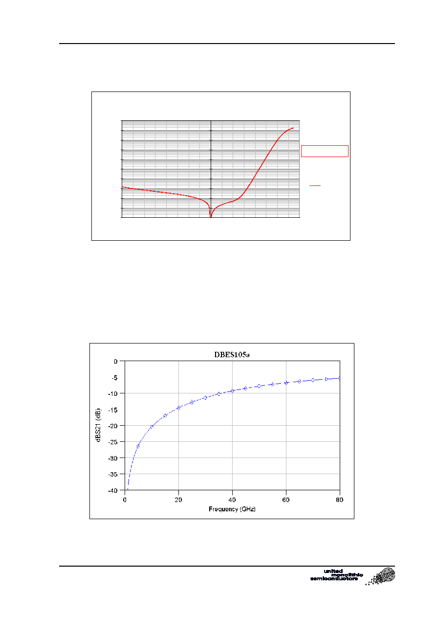
Typical DC Measurements
Typical On-Wafer Measurements
Bias Conditions
Vak = 0V
UI-Characteristic
1E-11
1E-10
1E-09
1E-08
1E-07
1E-06
1E-05
1E-04
1E-03
1E-02
1E-01
0.00 0.25 0.50 0.75 1.00
Voltage U
D
[V]
C
u
rre
n
t
|I
D
|
[A
]
-4.0
-3.0
-2.0
-1.0
1x5µm
Is = 3.5e-14 A
DBES105a
Flip-Chip Dual Diode
Ref. : DSDBES1051067 -08-Mar-01
4/4
Specifications subject to change without notice
Route DÈpartementale 128 , B.P.46 - 91401 ORSAY Cedex - FRANCE
Tel.: +33 (0)1 69 33 03 08 - Fax : +33 (0)1 69 33 03 09
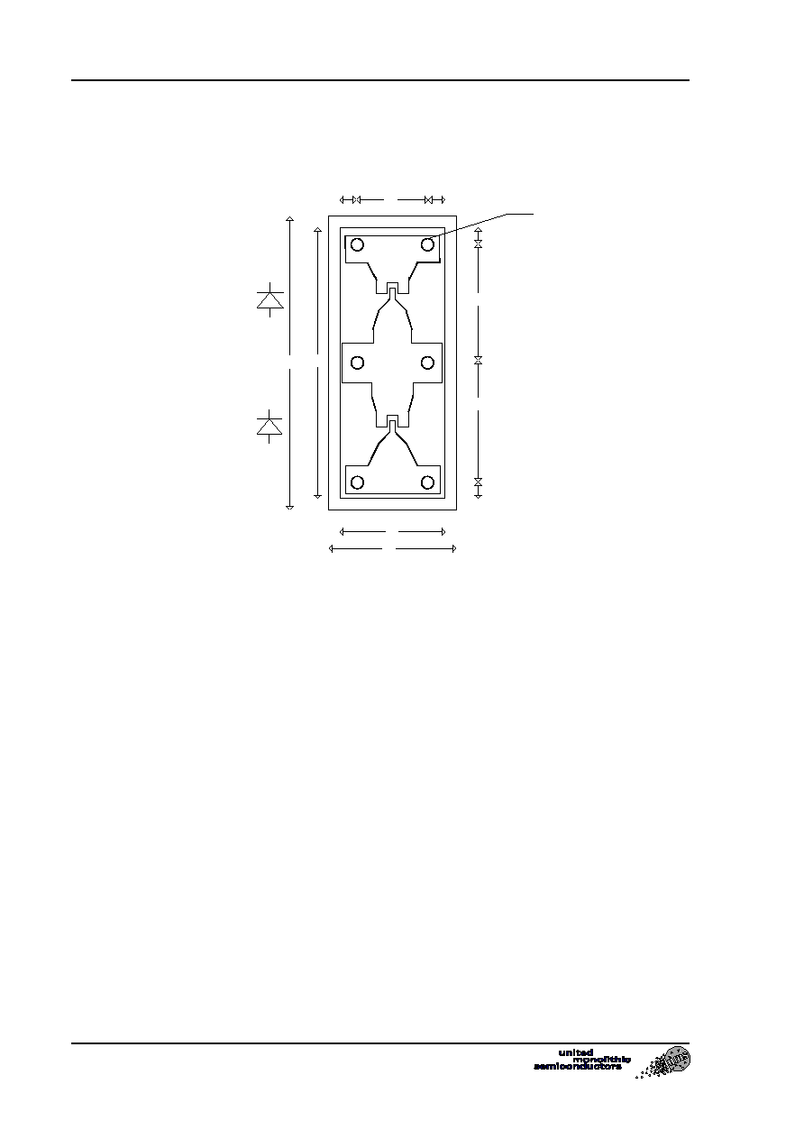
Mechanical data
Dimensions in µm
Dimensions: 230
±
35 x 530
±
35 µm
Thickness= 100µm
±
10 µm
Ordering Information
Chip form
:
DBES105a-99F/00
Information furnished is believed to be accurate and reliable. However United Monolithic Semiconductors
S.A.S. assumes no responsability for the consequences of use of such information nor for any infringement of
patents or other rights of third parties which may result from its use. No license is granted by implication or
otherwise under any patent or patent rights of United Monolithic Semiconductors S.A.S.. Specifications
mentioned in this publication are subject to change without notice. This publication supersedes and replaces all
information previously supplied. United Monolithic Semiconductors S.A.S. products are not authorised for use
as critical components in life support devices or systems without express written approval from United
Monolithic Semiconductors S.A.S.
53
0
46
0
30
30
100
160
230
20
4
20
4
26
diameter 20
26