 | –≠–ª–µ–∫—Ç—Ä–æ–Ω–Ω—ã–π –∫–æ–º–ø–æ–Ω–µ–Ω—Ç: US3004CW | –°–∫–∞—á–∞—Ç—å:  PDF PDF  ZIP ZIP |

US3004/US3005
4-1
Rev. 1.2
12/8/00
TYPICAL APPLICATION
TYPICAL APPLICATION
DESCRIPTION
DESCRIPTION
The US3004/5 series of controller ICs are specifically
designed to meet Intel specification for Pentium III
TM
microprocessor applications as well as the next genera-
tion P6 family processors. The IC provides a single
chip controller IC for the Vcore , GTL+ and clock
supplies required for the Pentium III applications.
These devices feature a patented topology that in
combination with a few external components as shown
in the typical application circuit ,will provide in excess of
20A of output current for an on- board DC/DC converter
while automatically providing the right output voltage via
the 5 bit internal DAC meeting the latest VRM specifica-
tion .These products also feature, loss less current sens-
ing by using the Rds-on of the high side Power
MOSFET as the sensing resistor, a Power Good win-
dow comparator that switches its open collector output
low when the output is outside of a
±
10% window. Other
features of the device are ; Undervoltage lockout for both
5V and 12V supplies, an external programmable soft
start function as well as programming the oscillator fre-
quency by using an external capacitor.
Meets Latest VRM 8.4 Specification for PIII
Provides Single Chip Solution for Vcore, GTL+
and Clock Supply
On board DAC programs the output voltage
from 1.3V to 3.5V. The US3004/5 remains on for
VID code of (11111).
Dual linear regulator controller on board for
1.5V GTL+ and 2.5V clock supplies
Loss less Short Circuit Protection
Synchronous operation allows maximum effi-
ciency
Patented architecture allows fixed frequency
operation as well as 100% duty cycle during
dynamic load
Min part count, No external Compensation
Soft Start
High current totem pole driver for direct driv-
ing of the external Power MOSFET
Power Good function
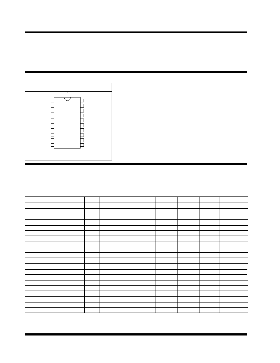
PACKAGE ORDER INFORMATION
PACKAGE ORDER INFORMATION
FEATURES
FEATURES
5 BIT PROGRAMMABLE SYNCHRONOUS BUCK
CONTROLLER IC WITH DUAL LDO CONTROLLER
APPLICATIONS
APPLICATIONS
Pentium III & next generation processor DC to DC
converter application
Low cost Pentium with AGP
Vout 3
5V
12V
VID0
3004app2-1.9
Vout 2
Vout 1
3.3V
Q2
C9
Q4
VID1
VID2
VID3
VID4
L1
L2
C5
R1
C3
C4
C6
Q1
R2
R3
C7
R4
C10
Q3
R7
R8
C11
R6
C12
C1
C2
C13
R9
R11
C15
R10
C14
R13
R12
R14
R15
12
HDrv
LDrv
Ct
SS
CS+
Gnd
Vfb3
D3
D2
D4
D1
D0
PGd
US3004
Lin1
Vfb1
CS-
V12
V5
Vfb2
Lin2
15
5
16
8
17
9
18
7
19
11
6
10
4
14
20
3
2
13
1
Power Good
R5
C8
3.3V
Ta (
∞
C)
Device Package 2.5V Output Voltage
0 TO 70
US3004CW 20 pin Plastic SOIC WB Adjustable
0 TO 70
US3005CW 20 pin Plastic SOIC WB Fixed
Notes: Pentium III is trade mark of Intel Corp.
4-2
Rev. 1.2
12/8/00
US3004,US3005
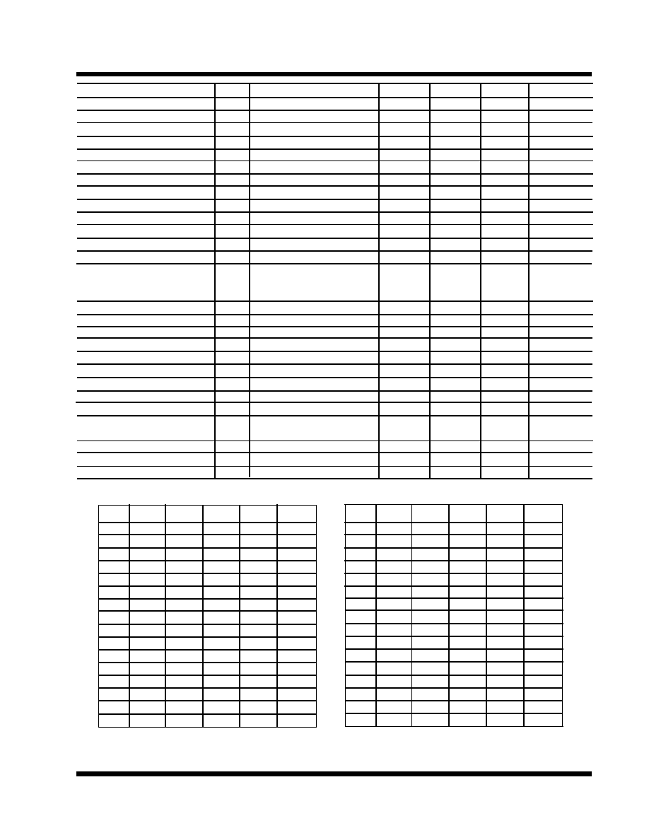
ELECTRICAL SPECIFICATIONS
ELECTRICAL SPECIFICATIONS
Unless otherwise specified ,these specifications apply over ,V
12
= 12V, V
5
= 5V and Ta=0 to 70
∞
C. Typical values
refer to Ta =25
∞
C. Low duty cycle pulse testing are used which keeps junction and case temperatures equal to the
ambient temperature.
ABSOLUTE MAXIMUM RATINGS
ABSOLUTE MAXIMUM RATINGS
V5 supply Voltage ........................................... 10V
V12 Supply Voltage ............................................ 20V
Storage Temperature Range ................................. -65 TO 150
∞
C
Operating Junction Temperature Range .......... 0 TO 125
∞
C
PACKAGE INFORMATION
PACKAGE INFORMATION
20 PIN WIDE BODY PLASTIC SOIC (W)
JA
=85
∞
C/W
4
3
2
1
7
6
5
18
19
20
TOP VIEW
11
13
12
14
10
15
9
16
8
17
Lin2
D0
D1
D2
D3
D4
Vfb3
SS
V12
LDrv
Ct / En
Lin1
Vfb1
Vfb2
V5
PGd
CS-
CS+
HDrv
Gnd
PARAMETER
SYM TEST CONDITION
MIN
TYP
MAX
UNITS
VID Section
DAC output voltage
0.99Vs
Vs
1.01Vs
V
(note 1)
DAC Output Line Regulation
0.1
%
DAC Output Temp Variation
0.5
%
VID Input LO
0.4
V
VID Input HI
2
V
VID input internal pull-up
27
k
resistor to V5
Power Good Section
Under voltage lower trip point
Vout ramping down
0.89Vs
0.90Vs
0.91Vs
V
Under voltage upper trip point
Vout ramping up
0.92Vs
V
UV Hysterises
.015Vs
.02Vs
.025Vs
V
Over voltage upper trip point
Vout ramping up
1.09Vs
1.10Vs
1.11Vs
V
Over voltage lower trip point
Vout ramping down
1.08Vs
V
OV Hysterises
.015Vs
.02Vs
.025Vs
V
Power Good Output LO
RL=3mA
0.4
V
Power Good Output HI
RL=5K pull up to 5V
4.8
V
Soft Start Section
Soft Start Current
CS+ =0V , CS- =5V
10
uA
US3004/US3005
4-3
Rev. 1.2
12/8/00
UVLO Section
UVLO Threshold-12V
Supply ramping up
9.2
10
10.8
V
UVLO Hysterises-12V
0.3
0.4
0.5
V
UVLO Threshold-5V
Supply ramping up
4.1
4.3
4.5
V
UVLO Hysterises-5V
0.2
0.3
0.4
V
Error Comparator Section
Input bias current
2
uA
Input Offset Voltage
-2
+2
mV
Delay to Output
Vdiff=10mV
100
nS
Current Limit Section
C.S Threshold Set Current
160
200
240
uA
C.S Comp Offset Voltage
-5
+5
mV
Hiccup Duty Cycle
Css=0.1 uF
2
%
Supply Current
Operating Supply Current
CL=3000pF
V5
20
V12
14
mA
Output Drivers Section
Rise Time
CL=3000pF
70
100
nS
Fall Time
CL=3000pF
70
130
nS
Dead band Time
CL=3000pF
100
200
300
nS
Oscillator Section
Osc Frequency
Ct=150pF
190
220
250
Khz
Osc Valley
0.2
V
Osc Peak
V5
V
LDO Controller Section
Vfb1 & Vfb2 (US3004)
1.477
1.500
1.522
V
Vfb2 (US3005)
Vfb1 (US3005)
2.500
V
Input bias current
2
uA
Lin1 or Lin2 Drive Current
50
mA
Note 1: Vs refers to the set point voltage given in Table 1.
D4
D3
D2
D1
D0
Vs
D4
D3
D2
D1
D0
Vs
0
1
1
1
1
1.30
1
1
1
1
1
2.0
0
1
1
1
0
1.35
1
1
1
1
0
2.1
0
1
1
0
1
1.40
1
1
1
0
1
2.2
0
1
1
0
0
1.45
1
1
1
0
0
2.3
0
1
0
1
1
1.50
1
1
0
1
1
2.4
0
1
0
1
0
1.55
1
1
0
1
0
2.5
0
1
0
0
1
1.60
1
1
0
0
1
2.6
0
1
0
0
0
1.65
1
1
0
0
0
2.7
0
0
1
1
1
1.70
1
0
1
1
1
2.8
0
0
1
1
0
1.75
1
0
1
1
0
2.9
0
0
1
0
1
1.80
1
0
1
0
1
3.0
0
0
1
0
0
1.85
1
0
1
0
0
3.1
0
0
0
1
1
1.90
1
0
0
1
1
3.2
0
0
0
1
0
1.95
1
0
0
1
0
3.3
0
0
0
0
1
2.00
1
0
0
0
1
3.4
0
0
0
0
0
2.05
1
0
0
0
0
3.5
Table 1 - Set point voltage vs. VID codes
4-4
Rev. 1.2
12/8/00
US3004,US3005
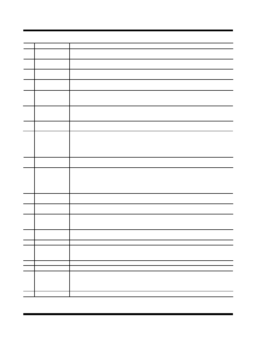
PIN DESCRIPTIONS
PIN DESCRIPTIONS
Pin Description
LSB input to the DAC that programs the output voltage. This pin can be pulled up exter-
nally by a 10k resistor to either 3.3V or 5V supply.
Input to the DAC that programs the output voltage.This pin can be pulled up externally by
a 10k
resistor to either 3.3V or 5V supply.
Input to the DAC that programs the output voltage.This pin can be pulled up externally by
a 10k resistor to either 3.3V or 5V supply.
MSB input to the DAC that programs the output voltage.This pin can be pulled up exter-
nally by a 10k resistor to either 3.3V or 5V supply.
This pin selects a range of output voltages for the DAC.When in the LOW state the range
is 1.3V to 2.05V. For VID codes of all "1" the US3004 keeps all the outputs on.
This pin is an open collector output that switches LO when the output of the converter is
not within
±
10% (typ) of the nominal output voltage.When PWRGD pin switches LO the
sat voltage is less than 0.4V at 3mA.
This pin is connected directly to the output of the Core supply to provide feedback to the
Error comparator.
This pin is connected to the Drain of the power MOSFET of the Core supply and it
provides the positive sensing for the internal current sensing circuitry. An external resis-
tor programs the C.S threshold depending on the Rds of the power MOSFET. An external
capacitor is placed in parallel with the programming resistor to provide high frequency
noise filtering.
This pin is connected to the Source of the power MOSFET for the Core supply and it
provides the negative sensing for the internal current sensing circuitry.
This pin provides the soft start for the switching regulator. An internal current source
charges an external capacitor that is conected from this pin to the GND which ramps up
the outputs of the switching regulator, preventing the outputs from overshooting as wellas
limiting the input current. The second function of the Soft Start cap is to provide long off
time (HICCUP) for the synchronous MOSFET during current limiting.
This pin programs the oscillator frequency in the range of 50 kHZ to 500kHZ with an
external capacitor connected from this pin to the GND.
This pin controls the gate of an external transistor for either the GTL+ linear regulator or
Clock supply.
This pin provides the feedback for the linear regulator that its output drive is Lin1 pin. For
US3005, this pin is connected to the 2.5V regulator, eliminating the external di-
viders.
This pin controls the gate of an external transistor for either the GTL+ linear regulator or
Clock supply.
This pin provides the feedback for the linear regulator that its output drive is Lin2 pin.
This pin serves as the ground pin and must be conected directly to the ground plane. A
high frequency capacitor (0.1 to 1 uF) must be connected from V5 and V12 pins to this
pin for noise free operation.
Output driver for the synchronous power MOSFET.
Output driver for the high side power MOSFET.
This pin is connected to the 12 V supply and serves as the power Vcc pin for the output
drivers.A high frequency capacitor (0.1 to 1 uF) must be connected directly from this pin
to GND pin in order to supply the peak current to the power MOSFET during the transi-
tions.
5V supply voltage.
PIN# PIN SYMBOL
19
D0
18
D1
17
D2
16
D3
15
D4
6
PGd
14
Vfb3
8
CS+
7
CS-
13
SS
1
Ct
2
Lin1
3
Vfb1
20
Lin2
4
Vfb2
10
Gnd
11
LDrv
9
HDrv
12
V12
5
V5
US3004/US3005
4-5
Rev. 1.2
12/8/00
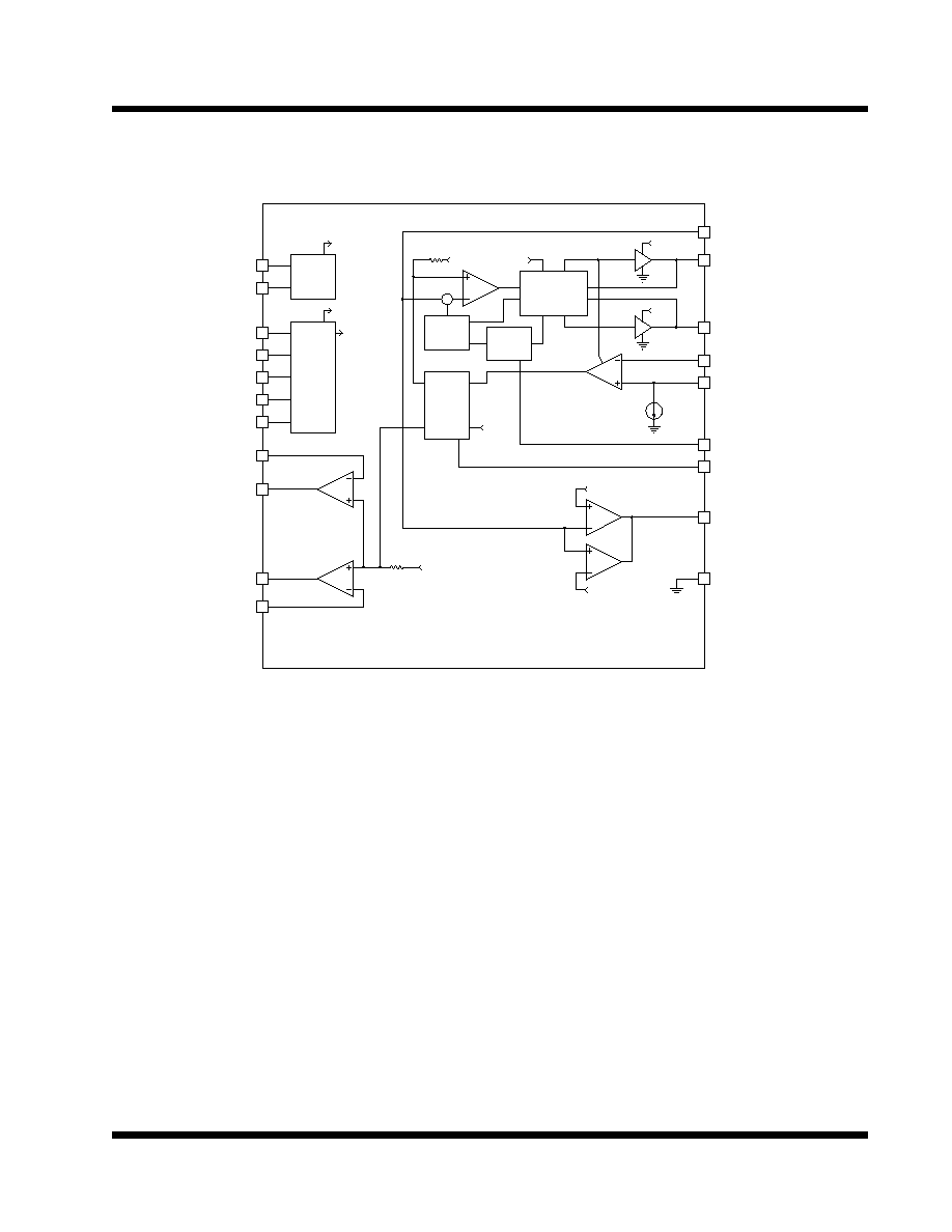
BLOCK DIAGRAM
BLOCK DIAGRAM
Figure 1 - Simplified block diagram of the US3004.
PWM
Control
V12
V12
3004blk2-1.3
Osc
Slope
Comp
+
1.5V
5Bit
DAC,
Ctrl
Logic
Enable
Soft
Start &
Fault
Logic
200uA
0.9Vset
1.1Vset
Vset
Enable
UVLO
Vset
Enable
Vfb1
Lin1
Lin2
Vfb2
D4
V5
V12
SS
Gnd
PGd
CS-
Ct / En
CS+
LDrv
HDrv
Vfb3
D3
D2
D1
D0
Over
Current
Enable