
UNISONIC TECHNOLOGIES CO., LTD
MJE13003
NPN EPITAXIAL SILICON TRANSISTOR
www.unisonic.com.tw
1 of 7
Copyright © 2005 Unisonic Technologies Co., Ltd
QW-R204-004,E
NPN SILICON POWER
TRANSISTORS
DESCRIPTION
These devices are designed for high≠voltage, high≠speed
power switching inductive circuits where fall time is critical. They
are particularly suited for 115 and 220V SWITCHMODE .
FEATURES
* Reverse Biased SOA with Inductive Load @ Tc=100
* Inductive Switching Matrix 0.5 ~ 1.5 Amp, 25 and 100
Typical tc = 290ns @ 1A, 100.
* 700V Blocking Capability
APPLICATIONS
* Switching Regulator's, Inverters
* Motor Controls
* Solenoid/Relay drivers
* Deflection circuits
TO-126
1
*Pb-free plating product number: MJE13003L
ORDERING INFORMATION
Order Number
Pin Assignment
Normal
Lead Free Plating
Package
1 2 3
Packing
MJE13003-x-T60-F-K MJE13003L-x-T60-F-K TO-126
B C E
Bulk
Note: x: Rank, refer to Classification of h
FE1
.
MJE13003L-x-T60-F-K
(1)Packing Type
(3)Package Type
(4)Rank
(5)Lead Plating
(2)Pin Assignment
(1)K: Bulk
(2) refer to Pin Assignment
(3) T60: TO-126
(4) x: refer to Classification of h
FE1
(5) L: Lead Free Plating, Blank: Pb/Sn

MJE13003
NPN EPITAXIAL SILICON TRANSISTOR
UNISONIC TECHNOLOGIES CO., LTD
2 of 7
www.unisonic.com.tw
QW-R204-004,E
ABSOLUTE MAXIMUM RATINGS
PARAMETER SYMBOL
RATINGS
UNIT
Collector-Emitter Voltage
V
CEO(SUS)
400 V
Collector-Emitter Voltage
V
CEO
700 V
Emitter Base Voltage
V
EBO
9 V
Continuous
I
C
1.5
Collector Current
Peak (1)
I
CM
3
A
Continuous
I
B
0.75
Base Current
Peak (1)
I
BM
1.5
A
Continuous
I
E
2.25
Emitter Current
Peak (1)
I
EM
4.5
A
Total Power Dissipation (T
C
=25)
P
D
40 W
Junction Temperature
T
J
150
Storage Temperature
T
STG
-40 ~ +150
Note Absolute maximum ratings are those values beyond which the device could be permanently damaged.
Absolute maximum ratings are stress ratings only and functional device operation is not implied.
ELECTRICAL CHARACTERISTICS
(T
C
=25∞C, unless otherwise specified.)
PARAMETER SYMBOL
TEST
CONDITIONS
MIN
TYP
MAX UNIT
OFF CHARACTERISTICS (Note)
Collector-Emitter Sustaining Voltage
V
CEO(SUS)
I
C
=10 mA , I
B
=0 400
V
T
C
=25∞C
1
Collector Cutoff Current
I
CEO
V
CEO
=Rated Value,
V
BE(OFF)
=1.5 V
T
C
=100
5
mA
Emitter Cutoff Current
I
EBO
V
EB
=9 V, I
C
=0
1
mA
SECOND BREAKDOWN
Second Breakdown Collector Current
with bass forward biased
Is/b
See Figure 5
Clamped Inductive SOA with base
reverse biased
RBSOA
See Figure 6
ON CHARACTERISTICS (Note)
h
FE1
I
C
=0.5A, V
CE
=10V 8
40
DC Current Gain
h
FE2
I
C
=1A, V
CE
=2V 5
25
I
C
=0.5A, I
B
=0.1A
0.5
I
C
=1A, I
B
=0.25A
1
I
C
=1.5A, I
B
=0.5A
3
Collector-Emitter Saturation Voltage
V
CE(SAT
)
I
C
=1A, I
B
=0.25A, T
C
=100
1
V
I
C
=0.5A, I
B
=0.1A
1
I
C
=1A, I
B
=0.25A
1.2
Base-Emitter Saturation Voltage
V
BE(SAT)
I
C
=1A, I
B
=0.25A, T
C
=100
1.1
V
DYNAMIC CHARACTERISTICS
Current-Gain-Bandwidth Product
f
T
I
C
=100mA, V
CE
=10V, f=1MHz
4
10
MHz
Output Capacitance
Cob
V
CB
=10V, I
E
=0,
f=0.1MHz
21 pF
SWITCHING CHARACTERISTICS
Resistive Load (Table 1)
Delay Time
t
D
0.05
0.1
s
Rise Time
t
R
0.5
1
s
Storage Time
t
S
2
4
s
Fall Time
t
FALL
V
CC
=125V, I
C
=1A, I
B1
=I
B2
=0.2A,
t
P
=25s, Duty Cycle1%
0.4
0.7
s
Inductive Load, Clamped (Table 1)
Storage Time
t
SV
1.7
4
s
Crossover Time
t
C
0.29
0.75
s
Fall Time
t
FALL
I
C
=1A, Vclamp=300V, I
B1
=0.2A,
V
BE(OFF)
=5Vdc, T
C
=100
0.15 s
Note: Pulse Test : PW=300s, Duty Cycle2%

MJE13003
NPN EPITAXIAL SILICON TRANSISTOR
UNISONIC TECHNOLOGIES CO., LTD
3 of 7
www.unisonic.com.tw
QW-R204-004,E
CLASSIFICATION OF h
FE1
RANK A B C D E F
RANGE
8 ~ 16
15 ~ 21
20 ~ 26
25 ~ 31
30 ~ 36
35 ~ 40
Table 1.Test Conditions for Dynamic Performance
Reverse Bias Safe Operating Area and Inductive Switching
Resistive
Switching
Test Circuits
P
w
5V
DUTY CYCLE10%
t
R
, t
F
10ns
68
0.001F
1k
1N4933
0.02F 270
+5V
1k
1k
33 1N4933
1N4933
33
+5V
R
B
MJE210
I
B
2N2222
2N2905
47
1/2W
100
MJE200
-V
BE
(
OFF
)
T.U.T.
Vcc
MR826*
V
clamp
*SELECTED FOR1kV
5.1k
51
V
CE
L
Ic
NOTE
P
W
and Vcc Adjusted for Desired Ic
R
B
Adjusted for Desired I
B1
+125V
R
B
D1
-4.0V
SCOPE
Rc
TUT
Circuit Values
Coil Data : GAP for 30 mH/2 A
V
CC
=20V
Ferroxcube core #6656 Lcoil=50mH
Vclamp=300V
Full Bobbin ( ~ 200 Turns) #20
V
CC
=125V
R
C
=125
D1=1N5820 or
Equiv.
R
C
=47
Test Waveforms
Output Waveforms
Ic
Ic(pk)
tf CLAMPED
t
tf
t1
V
CE
TIME
t2
t
V
CE
or
Vclamp
t1 Adjusted to
Obtain Ic
Test Equipment
Scope-Tektronics
475 or Equivalent
t1
Lcoil(Icpk)
Vcc
t2
Lcoil(Icpk)
Vclamp
+10.3 V
25S
0
-8.5V
tr, tf<10ns
Duty Cycly=1.0%
R
B
and Rc adjusted
for desired I
B
and Ic
Figure 1. Inductive Switching Measurements
Time
I
CPK
90% V
clamp
I
C
t
sv
t
RV
t
FI
t
TI
V
clamp
10% V
clamp
t
c
90% Ic
2% Ic
10%
Icpk
V
CE
I
B
90% I
B1
Ic
AMP
Tc
t
sv
s
t
RV
s
t
FI
s
t
TI
s
t
c
s
0.5
1
1.5
25
100
1.3
1.6
0.23
0.26
0.30
0.30
0.35
0.40
0.30
0.36
25
100
1.5
1.7
0.10
0.13
0.14
0.26
0.05
0.06
0.16
0.29
25
100
1.8
3
0.07
0.08
0.10
0.22
0.05
0.08
0.16
0.28
Table 2. Typical Inductive Switching Performance
NOTE: All Data Recorded in the Inductive Switching
Circuit in Table 1

MJE13003
NPN EPITAXIAL SILICON TRANSISTOR
UNISONIC TECHNOLOGIES CO., LTD
4 of 7
www.unisonic.com.tw
QW-R204-004,E
SWITCHING TIMES NOTE
In resistive switching circuits, rise, fall, and storage times have been defined and apply to both current and voltage
waveforms since they are in phase. However, for inductive loads, which are common to SWITCHMODE power
supplies and hammer drivers, current and voltage waveforms are not in phase. Therefore, separate measurements
must be made on each waveform to determine the total switching time. For this reason, the following new terms
have been defined.
t
SV
= Voltage Storage Time, 90% I
B1
to 10% Vclamp
t
RV
= Voltage Rise Time, 10 ~ 90% Vclamp
t
FI
= Current Fall Time, 90 ~ 10% I
C
t
TI
= Current Tail, 10 ~ 2% I
C
t
C
= Crossover Time, 10% Vclamp to 10% I
C
For the designer, there is minimal switching loss during storage time and the predominant switching power losses
occur during the crossover interval and can be obtained using the standard equation from AN≠222:
PSWT = 1/2 V
CC
I
C
(t
C
)f
In general, t
RV
+ t
FI
t
C
. However, at lower test currents this relationship may not be valid.
As is common with most switching transistors, resistive switching is specified at 25 and has become a
benchmark for designers. However, for designers of high frequency converter circuits, the user oriented
specifications which make this a "SWITCHMODE" transistor are the inductive switching speeds (t
C
and t
SV
) which
are guaranteed at 100.
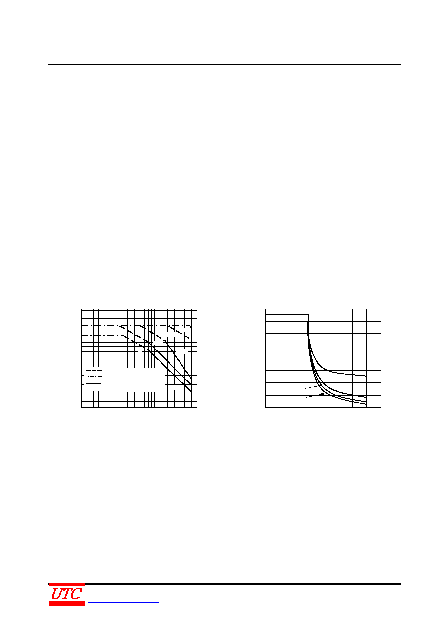
RESISTIVE SWITCHING PERFORMANCE
T
i
m
e
,
t
(
£
g
s
)
0.02
Figure 2. Turn-On Time
0.05
0.5
2
1
0.7
0.2
0.1
0.02
0.1
0.2
0.3
Collector Current, I
C
(A)
t
R
20
t
D
@ V
BE(OFF)
=5V
Vcc=125V
Ic/I
B
=5
T
J
=25
0.07
T
i
m
e
,
t
(
£
g
s
)
0.02
Figure 3. Turn-Off Time
0.05
1
10
7
2
1
0.5
0.2
0.1
0.2
0.5
2
0.3
0.1
t
s
0.5
0.3
0.05
0.03
0.03
0.07
0.7 10
Vcc=125V
Ic/I
B
=5
T
J
=25
t
F
5
3
0.7
0.03
0.07
0.3
0.7
E
f
f
e
c
t
i
v
e
T
r
a
n
s
i
e
n
t
T
h
e
r
m
a
l
R
e
s
i
s
t
a
n
c
e
,
R
(
t
)
(
N
o
r
m
a
l
i
z
e
d
)
0.01
Figure 4. Thermal Response
0.02
2
1
0.7
0.5
0.1
0.07
0.01
0.1
0.05
0.2
0.5
Time or Pulse Width, t (ms)
1
0.3
0.2
0.05
0.03
0.02
5
10
20
50
100
200
500
1000
P
(PK)
t
1
t
2
Duty Cycle, D=t
1
/t
2
Z
JC(t)
=r(t) R
JC
R
JC
=3.12/W Max
D Curves Apply for Power
Pulse Train Shown
Read Time at t1
T
J(pk)
-TC=P
(pk)
P
JC(t)
D=0.5
0.2
0.1
0.05
0.02
0.01
Single Pulse
0.03
0.3
3
Collector Current, I
C
(A)
MJE13003
NPN EPITAXIAL SILICON TRANSISTOR
UNISONIC TECHNOLOGIES CO., LTD
5 of 7
www.unisonic.com.tw
QW-R204-004,E
SAFE OPERATING AREA INFORMATION
FORWARD BIAS
There are two limitations on the power handling ability of a transistor: average junction temperature and second
breakdown. Safe operating area curves indicate I
C
-V
CE
limits of the transistor that must be observed for reliable
operation; i.e., the transistor must not be subjected to greater dissipation than the curves indicate.
The data of Figure 5 is based on T
C
= 25; T
J(PK)
is variable depending on power level. Second breakdown pulse
limits are valid for duty cycles to 10% but must be derated when T
C
25. Second breakdown limitations do not
derate the same as thermal limitations. Allowable current at the voltages shown on Figure 5.
T
J(PK)
may be calculated from the data in Figure 4. At high case temperatures, thermal limitations will reduce the
power that can be handled to values less than the limitations imposed by second breakdown.
REVERSE BIAS
For inductive loads, high voltage and high current must be sustained simultaneously during turn-off, in most cases,
with the base to emitter junction reverse biased. Under these conditions the collector voltage must be held to a safe
level at or below a specific value of collector current. This can be accomplished by several means such as active
clamping, RC snubbing, load line shaping, etc. The safe level for these devices is specified as Reverse Bias Safe
Operating Area and represents the voltage-current conditions during reverse biased turn-off. This rating is verified
under clamped conditions so that the device is never subjected to an avalanche mode. Figure 6 gives PBSOA
characteristics.
The Safe Operating Area of Figures 5 and 6 are specified ratings(for these devices under the test conditions shown.)
C
o
l
l
e
c
t
o
r
C
u
r
r
e
n
t
,
I
C
(
A
)
5
Figure 5. Active Region Safe Operating Area
200
10
5
2
1
0.5
0.1
20
100
Collector-Emitter Voltage, V
CE
(V)
0.2
0.05
0.02
0.01
10
50
500
1.0 ms
100s
5.0 ms
dc
Figure 6. Reverse Bias Safe Operating Area
Collector-Emitter Clamp Voltage,V
CE
(V)
V
BE(OFF)
=9V
T
J
100
I
B1
=1A
5V
C
o
l
l
e
c
t
o
r
C
u
r
r
e
n
t
,
I
C
(
A
)
3V
1.5V
1.6
1.2
0.8
0.4
0
0
100
200
300
400
500
600
700
800
10 ms
Thermal Limit(Single Pule)
Bonding Wire Limit
Second Breakdown Limit
Curves Apply Below Rated
V
CEO
Tc=25
300

MJE13003
NPN EPITAXIAL SILICON TRANSISTOR
UNISONIC TECHNOLOGIES CO., LTD
6 of 7
www.unisonic.com.tw
QW-R204-004,E
TYPICAL PERFORMANCE CHARACTERISTICS
D
C
C
u
r
r
e
n
t
G
a
i
n
,
h
F
E
0.02
DC Current Gain
0.03
0.05
2
80
60
40
30
20
1
0
8
4
0.1
0.2
0.3
0.5 0.7
Collector Current,I
C
(A)
C
o
l
l
e
c
t
o
r
-
E
m
i
t
t
e
r
V
o
l
t
a
g
e
,
V
C
E
(
V
)
0.002
Collector Saturation Region
0.005 0.01
1
2
1.6
1.2
0.8
0.4
0
0.02
0.05
0.1
0.2
0.5
Base Current, I
B
(A)
2
V
CE
=2V
- - - - - -V
CE
=5V
-55
25
T
J
=150
6
0.07
1
T
J
=25
1.5A
1A
0.5A
0.3A
Ic=0.1A
V
o
l
t
a
g
e
,
V
(
V
)
0.02
Base-Emitter Voltage
0.03
0.05
2
1.4
1.2
1
0.8
0.6
0.4
0.1
0.2
0.3
0.5 0.7
25
25
150
V
o
l
t
a
g
e
,
V
(
V
)
0.02
Collector-Emitter Saturation Region
0.03
0.05
0.5
0.35
0.25
0.2
0.15
0.05
0
0.1
0.2
0.3
1
2
Collector Current, I
C
(A)
25
V
BE(SAT)
@ I
C
/I
B
=3
- - - - - -V
BE(ON)
@ V
CE
=2V
T
J
=-55
150
T
J
=-55
Ic/I
B
=3
0.3
0.1
0.07
0.7
0.07
1
C
o
l
l
e
c
t
o
r
C
u
r
r
e
n
t
,
I
C
(
A
)
-0.4
Collector cut-off Region
-0.2
+0.6
0
+0.2
+0.4
Base-Emitter Voltage, V
BE
(V)
V
CE
=250V
100
T
J
=150
75
50
25
REVERSE
FORWARD
C
a
p
a
c
i
t
a
n
c
e
,
C
(
p
F
)
0.1
Capacitance
0.5
50
500
300
200
100
70
30
20
5
1
2
5
10 20
Reverse Voltage, V
R
(V)
100
1000
50
10
7
125
10
4
10
3
10
2
10
1
10
0
10
-1
Cib
Cob
T
J
=25
0.2
200 500
Collector Current,I
C
(A)

MJE13003
NPN EPITAXIAL SILICON TRANSISTOR
UNISONIC TECHNOLOGIES CO., LTD
7 of 7
www.unisonic.com.tw
QW-R204-004,E
UTC assumes no responsibility for equipment failures that result from using products at values that
exceed, even momentarily, rated values (such as maximum ratings, operating condition ranges, or
other parameters) listed in products specifications of any and all UTC products described or contained
herein. UTC products are not designed for use in life support appliances, devices or systems where
malfunction of these products can be reasonably expected to result in personal injury. Reproduction in
whole or in part is prohibited without the prior written consent of the copyright owner. The information
presented in this document does not form part of any quotation or contract, is believed to be accurate
and reliable and may be changed without notice.