
UTC TEA1062N / TEA1062AN
LINEAR INTEGRATED CIRCUIT
UTC
UNISONIC TECHNOLOGIES CO., LTD.
1
QW-R108-011,A
LOW VOLTAGE TELEPHONE
TRANSMISSION CIRCUIT WITH
DIALLER INTERFACE
DESCRIPTION
The UTC TEA1062N / TEA1062AN is a bipolar
integrated circuit performing all speech and line
interface function, required in the fully electronic
telephone sets. It performs electronic switching
between dialing speech. The circuit is able to
operate down to D.C. line voltage of 1.6V (with
reduced performance) to facilitate the use of more
telephone sets in parallel.
FEATURES
* Low d.c. line voltage; operates down to 1.6V
(excluding polarity guard).
*Voltage regulator with adjustment static resistance.
*Provides supply with limited current for external
circuitry.
*Symmetrical high-impedance inputs (64k
) for
dynamic, magnetic or piezoelectric microphones.
*Asymmetrical high-impedance inputs (32k
) for
electret microphones.
*DTMF signal input with confidence tone.
DIP-16
SOP-16
*Mute input for pulse or DTMF dialing.
*Receivering amplifier for several types of earphones.
*Large amplification setting range on microphone
and earpiece amplifiers.
*Line loss compensation facility , line current
depedant (microphone and earpiece amplifiers).
*Gain control adaptable to exchange supply.
*Possibility to adjust the d.c. line voltage.
QUICK REFERENCE DATA
Line voltage at I
line
=15mA
V
LN
typ. 3.8 V
Line current operating range[pin1]
normal operation
with reduced performance
I
line
I
line
11 to 140 mA
1 to 11 mA
Internal supply current
I
CC
typ. 1mA
Supply current for peripherials
at I
line
=15 mA MUTE input LOW(1062 is HIGH)
VCC>2.2V
VCC>2.8V
I
p
I
p
typ. 1.8mA
typ. 0.7mA
Voltage amplification range
microphone amplifier
receiving amplififer
A
VD
A
VD
44 to 52 dB
20 to 39 dB
Line loss compansation
Amplification control range
Exchange supply voltage range
Exchange feeding bridge resistance range
A
VD
V
exch
R
exch
typ. 6 dB
36 to 60V
400 to 1000
Operating ambient temperature range
T
amb
-25 to +75
�
C
UTC TEA1062N / TEA1062AN
LINEAR INTEGRATED CIRCUIT
UTC
UNISONIC TECHNOLOGIES CO., LTD.
2
QW-R108-011,A
dB
SUPPLY AND
REFERENCE
CONTROL
CURRENT
CURRENT
REFERENCE
LOW
VOLTAGE
CIRCUIT
2
3
16
8
15
14
9
12
11
6
7
10
13
1
5
4
REG
AGC
V
EE
MUTE
DTMF
MIC-
MIC+
IR
V
CC
LN
GAR
QR
GAS1
GAS2
SLPE
STAB
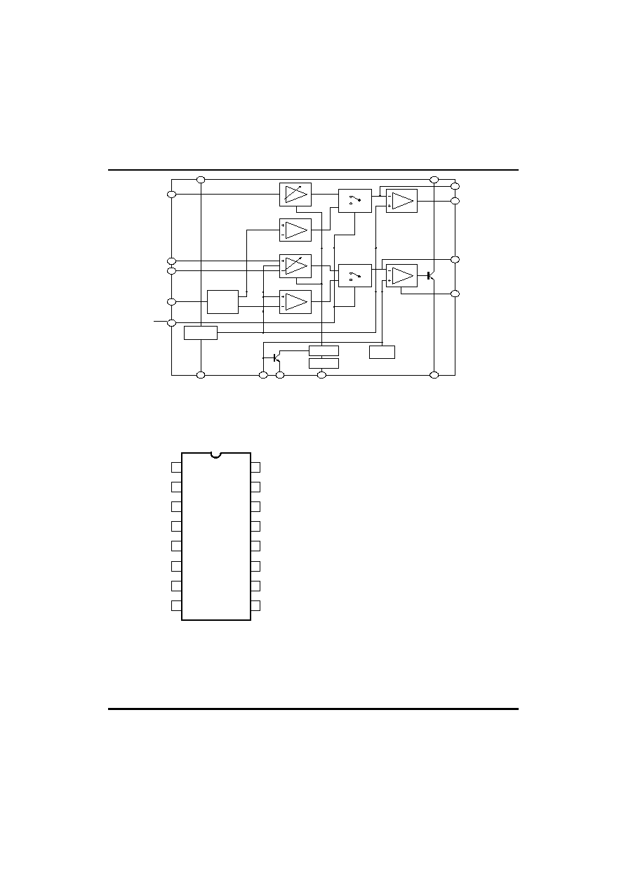
Fig.1 Block Diagram
1 LN positive line terminal
2 GAS1 gain adjustment; transmitting amplifier
3 GAS2 gain adjustment; transmitting amplifier
4 QR non-inverting output,receiving amplifier
5 GAR gain adjustment; receiving amplifier
6 MIC- inverting microphone input
7 MIC+ on-inverting microphone input
8 STAB current stabilizer
9 VEE negative line terminal
10 IR receiving amplifier input
11 DTMF dual-tone multi-frequency input
12 MUTE mute input
13 Vcc positive supply decoupling
14 REG voltage regulator decoupling
15 AGC automatic gain control input
16 SLPE slope (DC resistance) adjustment
Fig.2 PIN CONFIGURATIONS
1
2
3
4
5
6
7
8
16
15
14
13
12
11
10
9
LN
GAS1
GAS2
QR
GAR
MIC-
MIC+
STAB
V
EE
IR
DTMF
MUTE
V
CC
REG
AGC
SLPE

UTC TEA1062N / TEA1062AN
LINEAR INTEGRATED CIRCUIT
UTC
UNISONIC TECHNOLOGIES CO., LTD.
3
QW-R108-011,A
ABSOLUTE MAXIMUM RATINGS
PARAMETER TEST
CONDITIONS SYMBOL
MIN
MAX
UNIT
Positive Continuous Line Voltage
VLN
12
V
Repetitive Line Voltage During
Switch-On Or Line Interruption
VLN
13.2
V
Repetitive Peak Line Voltage for a 1 ms Pulse/5s
R10=13
R9=20
(see
Fig.15)
VLN
28
V
Line Current (1)
R9=20
Iline 140
mA
Voltage on All Other Pins
Vi
VCC+0.7
V
-Vi
0.7
V
Total Power Dissipation (2)
R9=20
Ptot 640
mW
Storage Temperature Range
Tstg
-40
+125
�
C
Operating Ambient Temperature Range
Tamb
-25
+75
�
C
Junction Temperature
Tj
+125
�
C
1. Mostly dependent on the maximum required T
amb
and the voltage between LN and SLPE (see Figs 6 ).
2. Calculated for the maximum ambient temperature specified T
amb
=75
�
C and a maximum junction temperature of
125
�
C.
THERMAL RESISTANCE
From junction to ambient in free air Rth j-a = 75K/W
ELECTRICAL CHARACTERISTICS
(Iline=11 to 140mA;V
EE
=0V;f=800Hz;T
amb
=25
�
C; unless otherwise
specified)
PARAMETER TEST
CONDITIONS
SYMBOL
MIN
TYP
MAX
UNIT
Supply; LN and VCC(pins 1 and 13)
Voltage Drop Over Circuit,
between LN and V
EE
MIC inputs open
I
line
=1mA V
LN
1.6
V
I
line
=4mA V
LN
1.9
V
I
line
=15mA V
LN
3.55
4.0
4.25 V
I
line
=100mA V
LN
4.9
5.7
6.5 V
I
line
=140mA V
LN
7.5
V
Variation with Temperature
I
line
=15mA
V
LN
/
T
-0.3
mV/K
Voltage Drop Over Circuit,
between LN and VEE with
External Resistor R
VA
I
line
=15mA
R
VA
(LN to REG)
=68k
3.5
V
I
line
=15mA
R
VA
(REG to SLPE)
=39k
4.5
V
Supply Current
V
CC
=2.8V I
CC
0.9 1.35 mA
Supply Voltage Available for
Peripheral Circuitry
I
line
=15mA
TEA1062N
I
p
=1.2mA; MUTE=HIGH
V
CC
2.2
2.7
V
l
p
=0mA;MUTE=HIGH V
CC
3.4
V
TEA1062AN
I
p
=1.2mA; MUTE=LOW
V
CC
2.2
2.7
V
l
p
=0mA;MUTE=LOW V
CC
3.4
V

UTC TEA1062N / TEA1062AN
LINEAR INTEGRATED CIRCUIT
UTC
UNISONIC TECHNOLOGIES CO., LTD.
4
QW-R108-011,A
ELECTRICAL CHARACTERISTICS
(continued)
PARAMETER TEST
CONDITIONS
SYMBOL
MIN
TYP
MAX
UNIT
Microphone inputs MIC+ and MIC- (pins 6 and 7)
Input impedance (differential)
between MIC- and MIC+
Z
i
64
k
Input impedance (sigle-ended)
MIC- or MIC+ to V
EE
Z
i
32
k
Common Mode Rejection Ratio
k
CMR
82
dB
Voltage Gain
MIC+ or MIC- to LN
I
line
=15mA
R7=68k
G
v
50.5
52.0 53.5
dB
Gain Variation with Frequency
at f=300Hz and f=3400Hz
w.r.t.800Hz
G
vf
+-0.2
dB
Gain Variation with Temperature
at -25
�
C and +75
�
C
w.r.t.25
�
C
without
R6;
I
line
=50mA
G
vT
+-0.2
dB
Dual-tone multi-frequency
input DTMF (pin 11)
Input impedance
Z
i
20.7 k
Voltage Gain from DTMF to LN
I
line
=15mA
R7=68k
G
v
24
25.5
27
dB
Gain Variation with Frequency
at f=300Hz and f=3400Hz
w.r.t.800Hz
G
vf
+-0.2 dB
Gain Variation with Temperature
at -25
�
C and +75
�
C
w.r.t.25
�
C
I
line
=50mA
G
vT
+-0.2 dB
Gain Adjustment GAS1 and GAS2 (pins 2 and 3)
Gain Variation of the Transmitting
Amplifier by Varying R7 between
GAS1 and GAS2
G
v
-8 0 dB
Sending Amplifier Output LN (pin 1)
Output Voltage
I
line
=15mA
THD=10%
V
LN
(rms)
1.7 2.3 V
I
line
=4mA
THD=10%
V
LN
(rms)
0.8 V
Noise output voltage
I
line
=15mA;
R7=68k
;
200
between
MIC- and MIC+;
psophometrically
weighted
V
NO
(rms)
-69
dBmp
Receiving Amplifier Input IR (pin 10)
Input impedance
Z
i
21 k
Receiving Amplifier Output QR (pin 4)
Output Impedance
Z
o
4
Voltage gain from IR to QR
I
line
=15mA;
R
L
(from pin 9 to
pin 4 )=300
G
v
29.5
31
32.5
dB
UTC TEA1062N / TEA1062AN
LINEAR INTEGRATED CIRCUIT
UTC
UNISONIC TECHNOLOGIES CO., LTD.
5
QW-R108-011,A
ELECTRICAL CHARACTERISTICS
(continued)
PARAMETER TEST
CONDITIONS
SYMBOL
MIN
TYP
MAX
UNIT
Gain Variation with Frequency
at f=300Hz and f=3400Hz
w.r.t.800Hz
G
vf
�
0.2
dB
Gain Variation with Temperature
at-25
�
C and +75
�
C
w.r.t.25
�
C
without R6
I
line
=50mA
G
vT
+-0.2 dB
Output Voltage
sinwave drive;
I
p
=0mA;THD=2%
R4=100k
I
line
=15mA
R
L
=150
V
O
(rms)
0.22
0.33 V
R
L
=450
V
O
(rms)
0.3 0.48
V
Output Voltage
THD=10%
R4=100k
R
L
=150
I
line
=4mA V
O
(rms)
15 mV
Noise Output Voltage
I
line
=15mA
R4=100k
IR
open-circuit
psophometrically
weighted
RL=300
V
NO
(rms)
50 V
Gain adjustment GAR (pin 5)
Gain Variation of Receiving
Amplifier Achievable by
Varying
R4 between GAR and QR
G
v
-11
0
dB
Mute Input (pin 12)
Input Voltage(HIGH)
V
IH
1.5 V
CC
V
Input Voltage(LOW)
V
IL
0.3
V
Input Current
I
MUTE
8 15
A
Reduction of Gain
MIC+ or MIC- to QR
MUTE=LOW
G
v
70 dB
Voltage Gain from DTMF to QR
MUTE=LOW
R4=100k
RL=300
G
v
-19 dB
Automatic Gain Control Input AGC
(
pin 15)
Controlling the Gain from lR to QR
and the Gain from MIC+/MIC-
to LN;R6 between AGC and VEE R6=110k
Gain Control Range
I
line
=70mA
G
v
-5.8
dB
Highest Line Current
for Maximum Gain
I
line
23
mA
Minimum Line Current
for Minimum Gain
I
line
61
mA