UTC M2904
LINEAR INTEGRATED CIRCUIT
UTC
UNISONIC TECHNOLOGIES CO., LTD.
1
QW-R105-024,A
SINGLE-SUPPLY DUAL
OPERATIONAL AMPLIFIER
DESCRIPTION
The UTC M2904 consists of two independent, high
gain, internally frequency compensated operation
amplifiers which were designed specifically to operate
from a single power supplies is also possible and the low
power supply current drain is independent of the
magnitude of the power supply voltage.
FEATURES
*Single Supply
*Operating Voltage: +3V~+32V
*Low Operating Current: 0.7mA (typ.)
*Slew Rate: 0.5V/s (typ.)
APPLICATIONS
*transducer amplifiers, DC gain blocks, and all the
conventional op amp circuits which now can be more
easily implemented in single power supply systems.
DIP-8
SOP-8
TSSOP-8
PIN CONFIGURATION
OUT1
IN1(-)
IN1(+)
GND
Vcc
+
OUT2
IN2(-)
IN2(+)
1
2
3
4
8
7
5
6
- +
+ -
UTC M2904
LINEAR INTEGRATED CIRCUIT
UTC
UNISONIC TECHNOLOGIES CO., LTD.
2
QW-R105-024,A
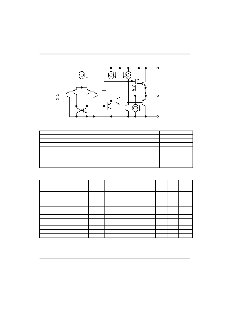
EQUIVALENT CIRCUIT (1/2 shown)
- INPUT
+ INPUT
GND
V
+
OUTPUT
ABSOLUTE MAXIMUM RATINGS
(Ta=25)
PARAMETER SYMBOL RATINGS
UNIT
Supply Voltage
V
+
(V
+
/V
-
) 32(
or�16)
V
Differential Input Voltage
V
ID
32
V
Input Voltage
V
IC
-0.3+32
V
Power Dissipation
DIP-8
SOP-8
TSSOP-8
P
D
500
300
300
mW
Operating Temperature Range
Topr
-40~+85
�C
Storage Temperature Range
Tstg
-50~+125
�C
ELECTRICAL CHARACTERISTICS
(Ta=25,V
+
=5V)
PARAMETER
SYMBOL
TEST
CONDITIONS MIN TYP MAX UNIT
Input Offset Voltage
V
IO
Rs=0
2 7 mV
Input Offset Current
I
IO
5 50 nA
Input Bias Current
I
B
25 250 nA
Large Signal Voltae Gain
Av
R
L
2k
100 dB
Maximum Output Voltage Swing
V
OM
R
L
=2k
3.5 V
Input Common Mode Voltage Range
V
ICM
0~3.5
V
Common Mode Rejection Ratio
CMR
85
dB
Supply Voltage Rejection Ratio
SVR
100
dB
Output Source Current
I
SOURCE
V
IN
+
=1V,V
IN
-
=0V
20 30 mA
Output Sink Current
I
SINK
V
IN
+
=0V,V
IN
-
=1V 8
20
mA
Channel Separation
CS
f=1k ~20kHz,Input Referred
120
dB
Operating Current
Icc
R
L
=
0.7
1.2 mA
Slew Rate
SR
V
+
/V
-
=�15V
0.5 V/s
Unity Gain Bandwidth
f
T
V
+
/V
-
=�15V
0.2 MHz
UTC M2904
LINEAR INTEGRATED CIRCUIT
UTC
UNISONIC TECHNOLOGIES CO., LTD.
3
QW-R105-024,A
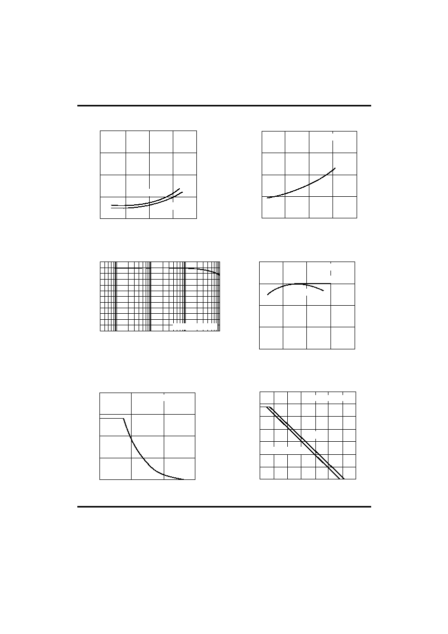
TYPICAL CHARACTERISTICS
Operating Current vs.Operating Voltage
Op
er
a
t
in
g
Cu
r
r
e
n
t , I
c
c
(mA)
Operating Voltage: V
+
(V)
0
Input Bias Current vs.Operating Voltage
In
p
u
t B
i
a
s
C
u
r
r
e
n
t
,
I
B
(n
A
)
10
25
100
75
50
0
20
30
40
0
Voltage Gain vs.Operating Voltage
O
p
e
n
Lo
op V
o
l
t
a
ge
G
a
i
n
,
A
v
(d
B
)
10
40
160
120
80
0
20
30
40
Operating Voltage: V
+
(V)
R
L
=20k
R
L
=2k
120
80
100
Frequency, f (Hz)
1k
C
h
a
n
n
e
l S
e
pa
r
a
ti
o
n
,
C
S
(d
B)
100
60
40
20
10k
100k
Channel Separation vs. Frequency
1k
M
a
x
i
m
u
m
O
u
t
p
ut
V
o
l
t
ag
e
S
w
i
n
g,
V
o
op
(
V
p
-
p)
10k
5
20
15
10
0
100k
1M
Frequency, f (Hz)
Maximum Output Voltage Swing vs.Frequency
O
p
e
n
Lo
op
Voltag
e
Ga
in,
Av
(
d
B
)
Frequency, f (Hz)
Open Loop Voltage Gain vs. Frequency
Ta=25
Operating Voltage: V
+
(V)
V
+
=5V,RL=2k
Ta=25
V
+
=15V,Ta=25
0
10
1
4
3
2
0
20
30
40
Ta=0 ~ +75
Ta= -20
1
10
80
140
120
100
0
100
1k
60
40
20
10k 100k 1M 10M
V =30V
+
V
+
=10~15V
RL= ,Ta=25

UTC M2904
LINEAR INTEGRATED CIRCUIT
UTC
UNISONIC TECHNOLOGIES CO., LTD.
4
QW-R105-024,A
29
-50
Ambient Temperature, Ta ()
0
M
a
x
i
mu
m Ou
t
p
ut
V
o
l
t
age
,
V
o
pp (V)
28
27
50
100
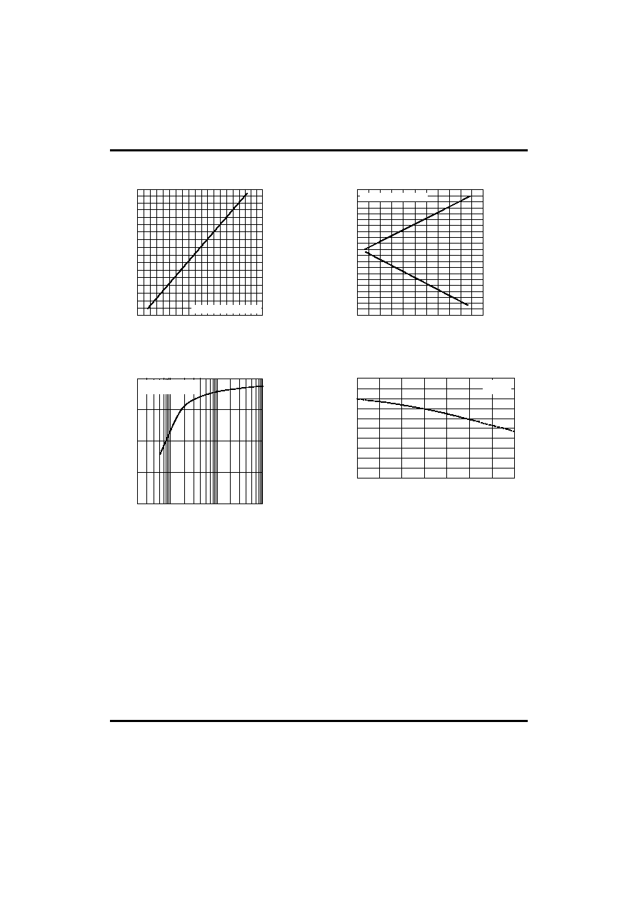
Maximum Output Voltage Swing vs. Temperature
150
4
-50
Ambient Temperature, Ta ()
-25
I
npu
t
O
f
f
s
et
V
o
l
t
age
,
V
i
o
(mV
)
2
0
0
25
50
-2
-4
75
100
125
Input Offset Voltage vs.Temperature
5
Sink Current, I
SINK
(A)
1
O
u
tp
ut Voltag
e
: V
o
(
V
)
4
3
10
100
2
1
1000
10000
Output Voltage vs.Sink Current
(1mA) (10mA)
0
5V
1V
-
+
Vo
I
SINK
O
per
at
i
ng
Cur
r
ent
,
I
c
c
(m
A
)
-50
0.8
1.4
1.2
1.0
0
-25
0
Ambient Temperature, Ta()
0.6
0.4
0.2
25
50
75 100 125
Operating Current vs.Temperature
90
-50
Ambient Temperature, Ta ()
-25
In
p
u
t
Bi
a
s
C
u
r
r
e
n
t
,
I
n
(
n
A)
80
70
0
25
50
60
50
75
100
125
Input Offset Voltage vs.Temperature
O
u
t
p
ut
V
o
l
t
age
f
r
om
O
p
e
r
at
i
ng
V
o
l
t
age
,
V
+
-V
o (V)
1
3
6
5
4
3
5
Source Current, I
SOURCE
(mA)
2
1
0
10
20 30 40
Source Current
1V
Vo
V =15V
+
V - Vo
+
+
-
40
30
20
10
0
V
+
=30V,RL=2k
V
+
=5V
V
+
=5V
V
+
=5V
V
+
=5V,Ta=25
V
+
=15V,Ta=25
UTC M2904
LINEAR INTEGRATED CIRCUIT
UTC
UNISONIC TECHNOLOGIES CO., LTD.
5
QW-R105-024,A
M
a
x
i
m
u
m
O
u
t
put
V
o
l
t
age
,
V
o
p
p
(V
)
10
30
20
10
0
20
30
40
Maximum Output Voltage
Operating Voltage, V
+
(V)
M
a
x
i
mu
m
O
u
tpu
t
Vo
l
t
ag
e
�
10
20
10
0
-10
Mazimum Output Voltage vs.Operating Voltage
Operating Voltage, V
+
/ V (V)
-
-20
0
�
20
M
a
x
i
m
u
m
Ou
t
put
V
o
l
t
age
,
V
o
pp (V
)
50
1
4
3
2
0
100
Load Resistance, R
L
()
200
5001k 2k
5k
Maximum Output Vltage Swing vs.LOad resistance
10k
4
-50
Ambient Temperature, Ta ()
-25
Inp
u
t O
ffs
e
t
Vo
l
t
ag
e,
V
IO
(m
V)
2
0
0
25
50
-2
-4
75
100
125
Input Offset Voltage vs.Temperature
RL=2k,Ta=25
RL=2k,Ta=25
+V
OM
(V)
- V
OM
(V)
V
+
=5V,Ta=25
V
+
=5V
APPLICATION
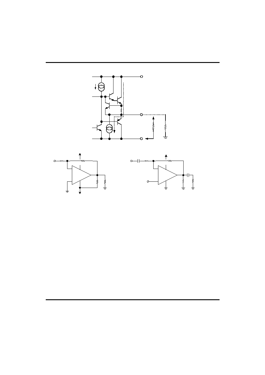
The UTC M2904, in its static state (No in and output condition) when design, Q
U
being biased by constant current
(break down beam) yet, Q
L
stays OFF.
While using with both power source mode, the cross-over distortion might occure instantly when Q
L
ON.
There might be cases when application for amplifier of audio signals, not only distortion but also the apparent
frequency bandwidth being narrowed remarkably. It is adjustable especially when using both power source mode,
constantly to use with higher on Q
U
than the load current (including feedback current),and then connect the
pull-down resister RP at the part between output and GND pins.
UTC M2904
LINEAR INTEGRATED CIRCUIT
UTC
UNISONIC TECHNOLOGIES CO., LTD.
6
QW-R105-024,A
Q
U
OUTPUT
Q
L
GND
Rp
R
L
V -
Improvement of Cross-over Distortion
Equivatent circuit at the output stage
Rs
IN
-
+
Rr
V+
Rp
R
L
V -
-
+
IN
Rs
Rr
Rp
R
L
V+
V+
Rp<R
L
// Rr