
UTC X0202/A
SCR
UTC
UNISONIC TECHNOLOGIES CO. LTD
1
QW-R301-006,A
SENSITIVE SCRs
DESCRIPTION
The X0202/A SCR series is suitable for all applications
where the available gate current is limited, such as ground
fault circuit interruptors, overvoltage crowbar protection in
low power supplies, capacitive ignition circuit,......
FEATURES:
*I
T(RMS) :
1.25A
*V
DRM
/V
RRM
:600/800V
SOT-223
3
2
1
4
1: GATE 2,4: ANODE 3: CATHODE
ABSOLUTE MAXIMUM RATINGS
(unless otherwise specified )
PARAMETERS SYMBOL
RATINGS
UNIT
Peak Repetitive Forward and Reverse Blocking Voltage
(Tj=110
�C, R
GK
=1k
)
X0202
X0202A
V
DRM
, V
RRM
600
800
V
RMS On-State Current (Ttab=95
�C)
180
�C conduction angle
I
T(RMS)
1.25
A
Average On-State Current (Ttab=95
�C)
180
�C conduction angle
IT
(AV)
0.8
A
Non Repetitive Surge Peak on-state Current
(tp=8.3ms Tj=25
�C)
I
TSM
25
A
Non Repetitive Surge Peak on-state Current
(tp=10ms Tj=25
�C)
I
TSM
22.5
A
I t Value for fusing (tp=10ms Tj=25
�C) I
t
2.5
A
2
S
Critical Rate Of Rise Of On-state Current
I
G
=2*I
GT
,tr100ns, f=60Hz, Tj=125
�C
dI/dt
50
A/
�s
Peak Gate Current (p=20
�s Tj=125�C) I
GM
1.2
A
Average Gate Power Dissipation (Tj=125
�C) P
G(AV)
0.2
W
Storage Junction Temperature Range
Tstg
-40~150
�C
Operating Junction Temperature Range
Tj
-40~125
�C
UTC X0202/A
SCR
UTC
UNISONIC TECHNOLOGIES CO. LTD
2
QW-R301-006,A
ELECTRICAL CHARACTERISTICS
(Tj=25
�C, unless otherwise specified)
PARAMETER SYMBOL
TEST
CONDITIONS
MIN
TYP
MAX
UNIT
Peak Forward or Reverse Blocking
Current Tj =25
�C
Tj =125
�C
I
DRM
, I
RRM
V
DRM
=V
RRM,
R
GK
=1k
5
500
� A
� A
Peak Forward On-State Voltage
V
TM
I
TM
= 2.5A, tp=380
�s
1.45
V
Gate Trigger Current
I
GT
VD=12V, RL=140
200
� A
Gate Trigger Voltage
V
GT
VD=12V, RL=140
0.8
V
Gate Non-Trigger Voltage
V
GD
V
D
=V
DRM,
R
L
=3.3k
,
R
GK
=1k
,
(Tj=125
�C)
0.1 V
Holding Current
I
H
I
T
=50mA, R
GK
=1k
5
mA
Latch Current
I
L
I
G
=1mA, R
GK
=1k
6
mA
Critical Rate of Rise of Off-State
Voltage
dv/dt
V
D
=67%V
DRM,
R
GK
=1k,
(Tj=110
�C)
10 V/
�s
Peak Reversed Gate Voltage
V
RG
I
RG
=10
� A
8 V
Threshold Voltage
V
TO
(Tj=125
�C)
0.9
V
Dynamic Resistance
Rd
(Tj=125
�C)
200
m
THERMAL CHARACTERISTICS
SYMBOL PARAMETER VALUE
UNIT
Rth(j-t)
Junction to tab
25
�C/W
Rth(j-a)
Junction to ambient
(S=5cm)
60
�C/W
S=Copper surface under tab
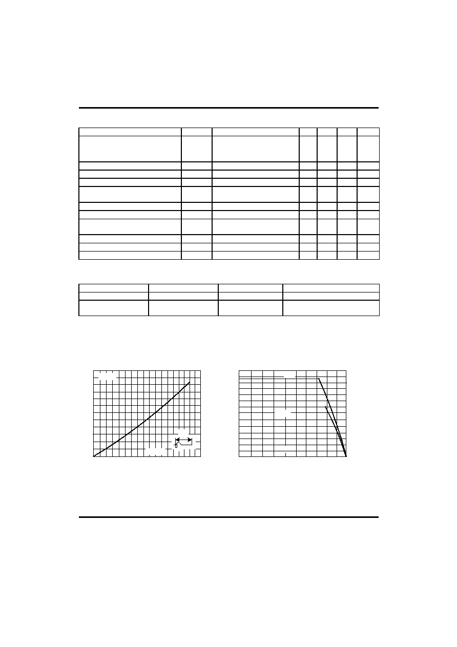
TYPICAL CHARACTERISTICS CURVE
Figure 1.Maximum Average Power Dissipation
vs. Average On-stage Current
0.0
0.2
0.1
0.3
0.4
0.6
0.8
0.2
0.0
0.4
0.5 0.6
0.7 0.8 0.9
1.0
1.2
=180�
P(W)
IT(av)(A)
360�
Figure 2-1.Average and D.C. On-state Current
vs.Lead Temperature
0
0.2
25
75
0.4
0.6
0.8
50
0.0
100
125
Ttab ()
1.0
1.2
1.4
IT(av)(A)
=180�
D.C.

UTC X0202/A
SCR
UTC
UNISONIC TECHNOLOGIES CO. LTD
3
QW-R301-006,A
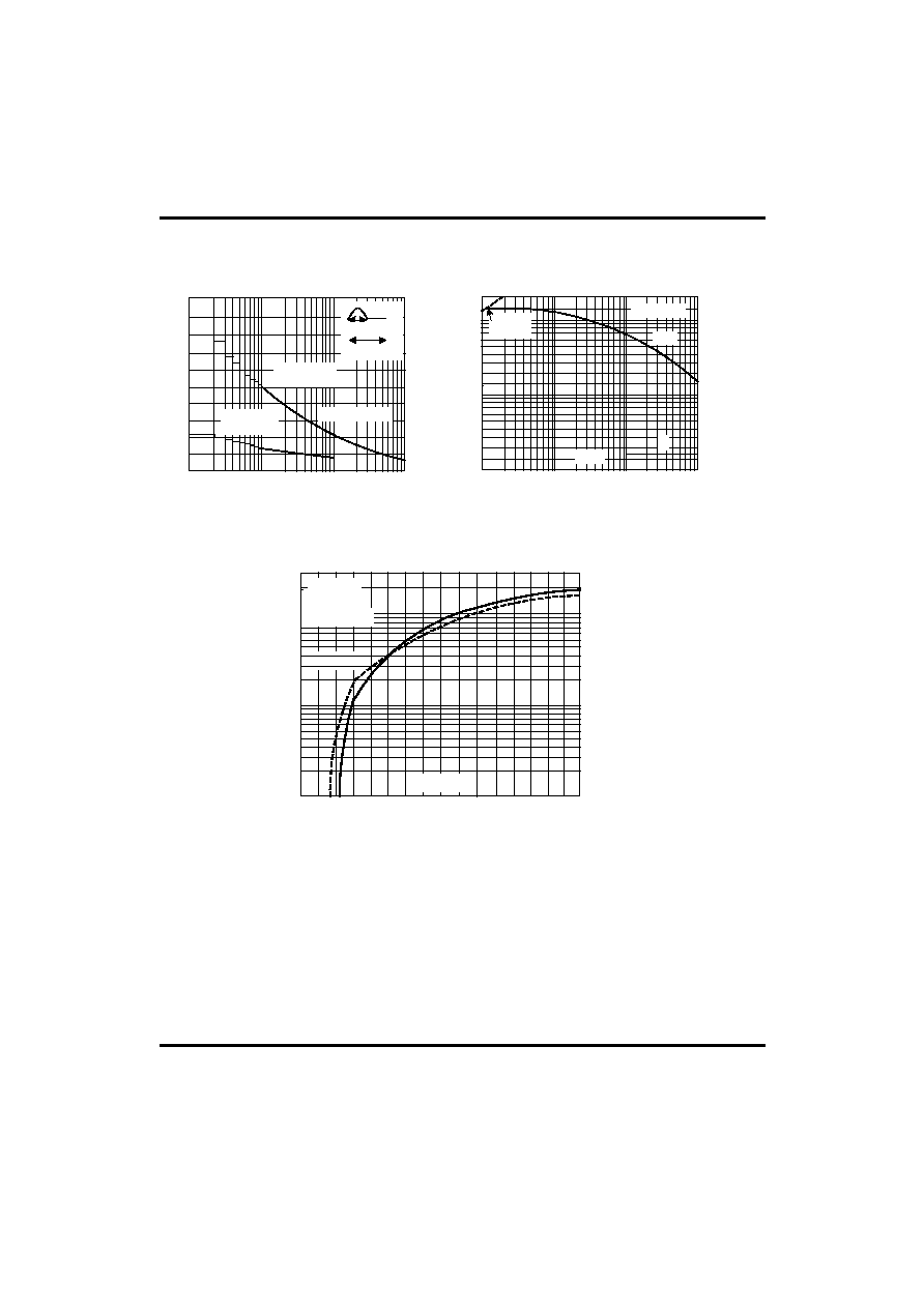
Figure 2-2.Average and D.C. On-state Current
vs.Ambient Temperature(Device Mounted On
FR4 with Recomended Pad Layout)
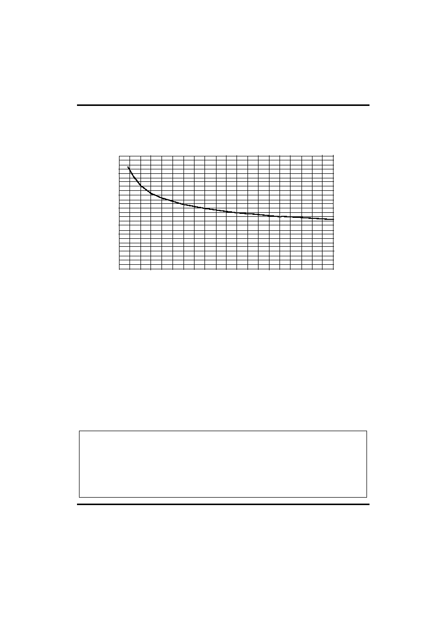
Figure 3. Relative Variation of Thermal
Impedance Junction to Ambient
vs.Pulse Duration
Tamb()
=180�
D.C.
0
25
75
50
100
125
0.2
0.4
0.6
0.8
0.0
1.0
1.2
1.4
1E-2
1E+1
1E+0
5E+2
1E+2
1E-1
0.01
0.1
1.0
tp(s)
Figure 4.Relative Variation of Gate Trigger
Current,Holding Current and Latching Current
Versus Junction Temperature (typical values).
-40
0.25
-20
20
0.50
0.75
1.00
0
0.0
40
60
80
100 120 140
1.25
1.50
Tj(
)
IGT,IH,IL[Tj]/GT,IH,IL[Tj]=25
IGT
IH&IL
(Rgk=1k
)
Figure 5.Relative Variation of Holding Current
vs.Gate-cathode Resistance (typical values).
1E-2
0.5
1E-1
1E+0
1.0
1.5
2.0
0.0
1E+1
2.5
3.0
3.5
4.0
IH[Rgk]/IH[Rgk=1k
]
Tj=25
Rgk(k
)
Figure 6.Relative Variation of dV/dt immunity
vs.Gate-Cathode Resistance (typical values).
0.0 0.2
0.6
1.0
0.4
0.1
0.8 1.0 1.2 1.4 1.6 1.8
10.0
Tj=125(
)
VD=0.67*VDRM
Rgk(k
)
2.0
dV/dt[Rgk]/dV/dt[Rgk=1k
]
Figure 7.Relative Variation of dV/dt Immunity
vs Gate-cathode Capacitance (typical values).
0
2
2
6
4
6
8
4
0
8
10 12 14 16 18
10
12
20 22
14
16
18
20
dV/dt[Rgk]/dV/dt[Rgk=1k
]
Cgk(nF)
Tj=125(
)
VD=0.67*VDRM
Rgk=1k
)
UTC X0202/A
SCR
UTC
UNISONIC TECHNOLOGIES CO. LTD
4
QW-R301-006,A
Figure 9.Non-repetitive Surge Peak on-state Current for
a Sinusoidal pulse with width tp<10ms,and
Corresponding Value of I t
0.01
0.10
10.00
1
1.00
10
100
300
Figure 8.Surge Peak On-state
Current vs.Number of Cycles.
1
5
10
100
10
15
20
1000
25
0
ITSM(A)
tp=10ms
one cycle
Tamb=25(
)
Repetitive
Tjinitial=25(
)
Nonrepetitive
Number of cycles
tp(ms)
I
2
t
ITSM
Tjinital=25
dI/dt
Limitation
ITSM(A),I
2
t(A
2
S)
Figure 10.On-state Characteristics (maximum values)
0.5
1.0
4.5
1E-1
3.0
1E+0
1E+1
3E+1
VTM(V)
TJ=TJ max
Tj max
Vto=0.9V
ITM(A)
1.5
2.5
2.0
3.5
4.0
Rd=200m
)
UTC X0202/A
SCR
UTC
UNISONIC TECHNOLOGIES CO. LTD
5
QW-R301-006,A
0.0
0.5
1.5
1.0
2.0
4.0
2.5
3.0
3.5
5.0
4.5
0
10
30
40
60
50
80
70
20
100
120
130
Rth(j-a) (/W)
90
110
Figure 11. Thermal resistance junction to ambient versus
copper surface under tab(Epoxy printed circuit board
FR4,copper thickness: 35m)
UTC assumes no responsibility for equipment failures that result from using products at values that
exceed, even momentarily, rated values (such as maximum ratings, operating condition ranges, or
other parameters) listed in products specifications of any and all UTC products described or contained
herein. UTC products are not designed for use in life support appliances, devices or systems where
malfunction of these products can be reasonably expected to result in personal injury. Reproduction in
whole or in part is prohibited without the prior written consent of the copyright owner. The information
presented in this document does not form part of any quotation or contract, is believed to be accurate
and reliable and may be changed without notice.