 | –≠–ª–µ–∫—Ç—Ä–æ–Ω–Ω—ã–π –∫–æ–º–ø–æ–Ω–µ–Ω—Ç: BUD700D | –°–∫–∞—á–∞—Ç—å:  PDF PDF  ZIP ZIP |

BUD700D
Vishay Telefunken
www.vishay.de
∑
FaxBack +1-408-970-5600
Rev. 1, 20≠Jan≠99
1 (8)
Document Number 86505
Silicon NPN High Voltage Switching Transistor
Features
D
Monolithic integrated C-E-free-wheel diode
D Simple-sWitch-Off Transistor (SWOT)
D HIGH SPEED technology
D Planar passivation
D 100 kHz switching rate
D Very low switching losses
D Very low dynamic saturation
D Very low operating temperature
D Optimized RBSOA
D High reverse voltage
Applications
Electronic lamp ballast circuits
94 8964
1
2
3
BUD700D
1 Base 2 Collector 3 Emitter
94 8965
2
1
3
BUD700D ≠SMD
1 Base 2 Collector 3 Emitter
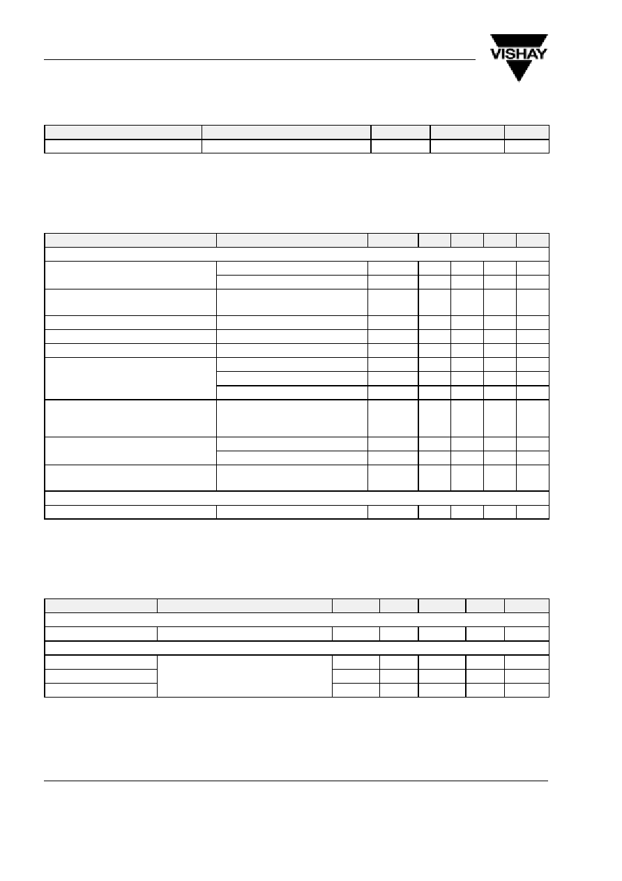
Absolute Maximum Ratings
T
case
= 25
∞
C, unless otherwise specified
Parameter
Test Conditions
Symbol
Value
Unit
Collector-emitter voltage
V
CEO
400
V
g
V
CEW
500
V
V
CES
700
V
Emitter-base voltage
V
EBO
11
V
Collector current
I
C
2
A
Collector peak current
I
CM
3
A
Base current
I
B
0.75
A
Base peak current
I
BM
1
A
Total power dissipation
T
case
50
∞
C
P
tot
20
W
Junction temperature
T
j
150
∞
C
Storage temperature range
T
stg
≠65 to +150
∞
C
BUD700D
Vishay Telefunken
www.vishay.de
∑
FaxBack +1-408-970-5600
Rev. 1, 20≠Jan≠99
2 (8)
Document Number 86505
Maximum Thermal Resistance
T
case
= 25
∞
C, unless otherwise specified
Parameter
Test Conditions
Symbol
Value
Unit
Junction case
R
thJC
5
K/W
Electrical Characteristics
T
case
= 25
∞
C, unless otherwise specified
Parameter
Test Conditions
Symbol
Min
Typ
Max
Unit
Transistor
Collector cut-off current
V
CE
= 700 V
I
CES
50
m
A
V
CE
= 700 V; T
case
= 150
∞
C
I
CES
0.5
mA
Collector-emitter breakdown
voltage (figure 1)
I
C
= 300 mA; L = 125 mH;
I
measure
= 100 mA
V
(BR)CEO
400
V
Emitter-base breakdown voltage
I
E
= 1 mA
V
(BR)EBO
11
V
Collector-emitter saturation voltage
I
C
= 0.3 A; I
B
= 0.1 A
V
CEsat
0.1
0.2
V
Base-emitter saturation voltage
I
C
= 0.3 A; I
B
= 0.1 A
V
BEsat
0.9
1
V
DC forward current transfer ratio
V
CE
= 2 V; I
C
= 10 mA
h
FE
10
V
CE
= 2 V; I
C
= 0.3 A
h
FE
10
V
CE
= 5 V; I
C
= 2 A
h
FE
4
6
Collector-emitter working voltage
V
S
= 50 V; L = 1 mH; I
C
= 2 A;
I
B1
= 0.7 A; ≠I
B2
= 0.2 A;
≠V
BB
= 5 V
V
CEW
500
V
Dynamic saturation voltage
I
C
= 1 A; I
B
= 0.2 A; t = 1
m
s
V
CEsatdyn
15
V
y
g
I
C
= 1 A; I
B
= 0.2 A; t = 3
m
s
V
CEsatdyn
4
V
Gain bandwidth product
I
C
= 200 mA; V
CE
= 10 V;
f = 1 MHz
f
T
4
MHz
Free-wheel diode
Forward voltage
I
F
= 0.7 A
V
F
1.2
V
Switching Characteristics
T
case
= 25
∞
C, unless otherwise specified
Parameter
Test Conditions
Symbol
Min
Typ
Max
Unit
Application specific switching time
measured with Nylos3
t
x
0.75
m
s
Resistive load (figure 2)
Turn on time
I
C
= 330 mA; I
B1
= 85 mA;
t
on
0.25
m
s
Storage time
C
B1
≠I
B2
= 170 mA; V
S
= 250 V
t
s
3
m
s
Fall time
t
f
0.4
m
s
BUD700D
Vishay Telefunken
www.vishay.de
∑
FaxBack +1-408-970-5600
Rev. 1, 20≠Jan≠99
3 (8)
Document Number 86505
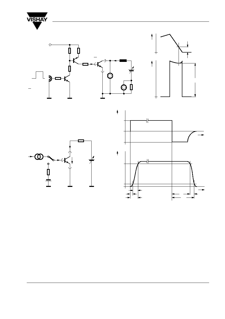
+
3 Pulses
94 8863
t
p
T +
0.1
t
p
+ 10 ms
V
S2
+ 10 V
I
B
w
I
C
5
I
C
L
C
V
S1
+
V
(BR)CEO
I
(BR)R
100 m
W
I
C
V
CE
V
(BR)CEO
I
measure
0 to 30 V
Figure 1. Test circuit for V
(BR)CE0
0
t
I
C
V
CE
R
C
V
CC
I
B
V
BB
R
B
I
B1
94 8852
+
(1)
(1) Fast electronic switch
I
B
I
B1
≠I
B2
I
C
0.9 I
C
0.1 I
C
t
t
s
t
off
t
f
t
r
t
d
t
on
Figure 2. Test circuit for switching characteristics ≠ resistive load
BUD700D
Vishay Telefunken
www.vishay.de
∑
FaxBack +1-408-970-5600
Rev. 1, 20≠Jan≠99
4 (8)
Document Number 86505
Typical Characteristics (T
case
= 25_C unless otherwise specified)
0
1
2
3
4
0
100
200
300
400
500
V
CE
≠ Collector Emitter Voltage ( V )
13723
I ≠ Collector Current (
A
)
C
0.1 x I
C
< I
B2
< 0.5 x I
C
V
CEsat
< 2 V
Figure 3. V
CEW
≠ Diagram
0
0.25
0.50
0.75
1.00
1.25
1.50
1.75
2.00
0
1
2
3
4
5
6
7
8
9 10 11 12
V
CE
≠ Collector Emitter Voltage ( V )
13725
I ≠ Collector Current (
A
)
C
I
B
=0.05A
0.1A
0.2A
0.15A
0.25A
Figure 4. I
C
vs. V
CE
1
10
100
0.01
0.10
1.00
10.00
I
C
≠ Collector Current ( A )
13727
h ≠ Forward DC Current
T
ransfer
Ratio
FE
5V
V
CE
=2V
10V
Figure 5. h
FE
vs. I
C
0.01
0.10
1.00
10.00
100.00
0
25
50
75
100
125
150
T
case
≠ Case Temperature (
∞
C )
13724
P
≠
T
otal Power Dissipation (
W
)
tot
12.5K/W
25K/W
50K/W
R
thJA
=135K/W
5K/W
Figure 6. P
tot
vs.T
case
0.01
0.10
1.00
10.00
0.01
0.10
1.00
10.00
I
B
≠ Base Current ( A )
13726
V
≠ Collector Emitter Saturation
V
oltage (
V
)
CEsat
I
C
=0.2A
2A
0.35A
1A
Figure 7. V
CEsat
vs. I
B
1
10
100
0.01
0.10
1.00
10.00
I
C
≠ Collector Current ( A )
13728
h ≠ Forward DC Current
T
ransfer
Ratio
FE
V
CE
=2V
T
j
= 125
∞
C
75
∞
C
25
∞
C
Figure 8. h
FE
vs. I
C
BUD700D
Vishay Telefunken
www.vishay.de
∑
FaxBack +1-408-970-5600
Rev. 1, 20≠Jan≠99
5 (8)
Document Number 86505
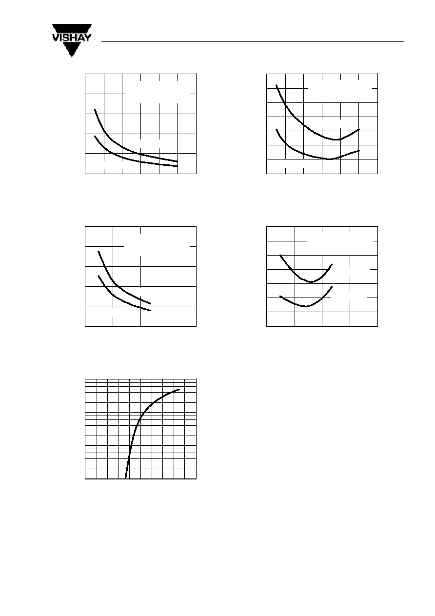
0
2
4
6
8
10
0
1
2
3
4
5
6
≠I
B2
/I
B1
13729
m
saturated switching
R-load
I
C
= 0.35A, I
B1
= 0.04A
T
case
= 25
∞
C
t ≠ Storage
T
ime ( s )
s
T
case
= 125
∞
C
Figure 9. t
s
vs. ≠I
B2
/I
B1
0
2
4
6
8
10
0
1
2
3
4
≠I
B2
/I
B1
13731
m
T
case
= 125
∞
C
saturated switching
R-load
I
C
= 0.35A, I
B1
= 0.085A
T
case
= 25
∞
C
t ≠ Storage
T
ime ( s )
s
Figure 10. t
s
vs. ≠I
B2
/I
B1
0.01
0.10
1.00
10.00
0
0.2 0.4 0.6 0.8 1.0 1.2 1.4 1.6 1.8 2.0
V
F
≠ Forward Voltage ( V )
13733
I ≠ Forward Current (
A
)
F
Figure 11. I
F
vs. V
F
0
0.1
0.2
0.3
0.4
0.5
0.6
0.7
0
1
2
3
4
5
6
≠I
B2
/I
B1
13730
m
T
case
= 125
∞
C
T
case
= 25
∞
C
t ≠ Fall
T
ime ( s )
f
saturated switching
R-load
I
C
= 0.35A, I
B1
= 0.04A
Figure 12. t
f
vs. ≠I
B2
/I
B1
0
0.1
0.2
0.3
0.4
0.5
0.6
0.7
0
1
2
3
4
≠I
B2
/I
B1
13732
m
T
case
= 125
∞
C
T
case
= 25
∞
C
t ≠ Fall
T
ime ( s )
f
saturated switching
R-load
I
C
= 0.35A, I
B1
= 0.085A
Figure 13. t
f
vs. ≠I
B2
/I
B1