Æ
CGP20 and DGP20
Vishay Semiconductors
formerly General Semiconductor
Document Number 88568
www.vishay.com
03-Jan-03
1
New Product
Miniature Clamper/Damper
Glass Passivated Rectifier
Reverse Voltage 1400 to 1500V
Forward Current 2.0A
Patented*
0.034 (0.86)
0.028 (0.71)
Dia.
0.140 (3.6)
0.104 (2.6)
Dia.
0.230 (5.8)
0.300 (7.6)
1.0 (25.4)
min.
1.0 (25.4)
min.
Maximum Ratings & Thermal Characteristics
Ratings at 25∞C ambient temperature unless otherwise specified.
Parameter
Symbol
CGP20
DGP20
Unit
Maximum repetitive peak reverse voltage
V
RRM
1400
1500
V
Maximum RMS voltage
V
RMS
980
1050
V
Maximum DC blocking voltage
V
DC
1400
1500
V
Maximum average forward rectified current
0.375" (9.5mm) lead length at T
A
= 50∞C
I
F(AV
)
2.0
A
Peak forward surge current 8.3ms single half sine
wave superimposed on rated load (JEDEC Method)
I
FSM
40
A
Maximum full load reverse current full cycle
average 0.375" (9.5mm) lead length at T
A
= 100∞C
I
R(AV)
200
µ
A
Typical thermal resistance
(Note 1)
R
JA
55
∞C/W
Operating junction and storage temperature range
T
J
, T
STG
≠65 to +175
∞C
Electrical Characteristics
Ratings at 25∞C ambient temperature unless otherwise specified.
Parameter
Symbol
CGP20
DGP20
Unit
Maximum instantaneous forward voltage at 2.0A
V
F
1.1
V
Maximum DC reverse current
T
A
= 25∞C
5.0
at rated DC blocking voltage
T
A
= 100∞C
I
R
100
µ
A
Maximum reverse recovery time at I
F
= 0.5A, I
R
= 50mA
t
rr
15
20
µ
s
Maximum reverse recovery time
typical
1.0
at I
F
=0.5A, I
R
=1.0A, I
rr
=0.25A
maximum
t
rr
1.5
µ
s
Typical junction capacitance at 4.0V, 1MHz
C
J
15
pF
Notes: (1) Thermal resistance from junction to ambient at 0.375" (9.5mm) lead length, P.C.B. mounted
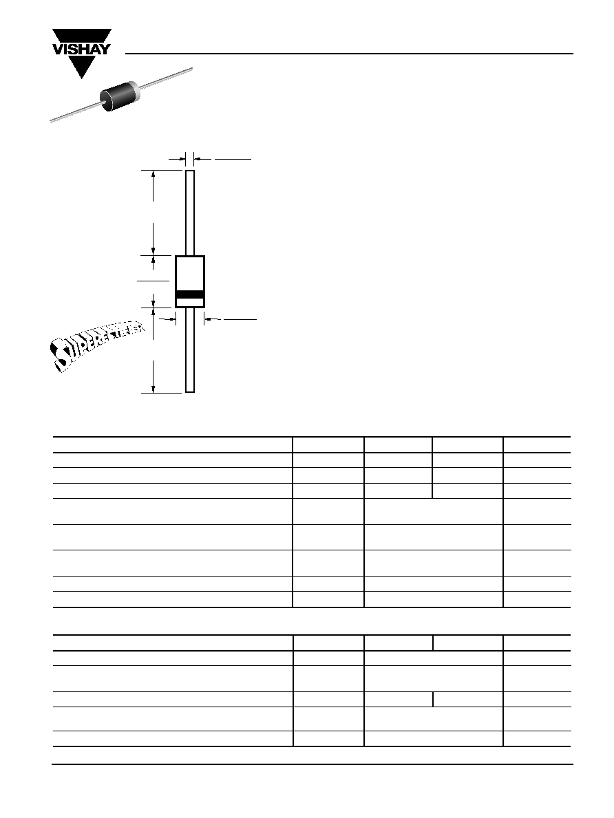
DO204AC (DO-15)
Features
∑ Specially designed for clamping circuits, horizontal
deflection systems and damper applications
∑ Plastic package has Underwriters Laboratory
Flammability Classification 94V-0.
∑ High temperature metallurgically bonded construction
∑ Cavity-free glass passivated junction
∑ 2.0 ampere operation at T
A
=50∞C with no thermal runaway
∑ Typical I
R
less than 0.1
µ
A
∑ Capable of meeting environmental standards of
MIL-S-19500
∑ High temperature soldering guaranteed: 350∞C/10 seconds,
0.375" (9.5mm) lead length, 5 lbs. (2.3kg) tension
Mechanical Data
Case: JEDEC DO-204AC, molded plastic over glass body
Terminals: Plated axial leads, solderable per
MIL-STD-750, Method 2026
Polarity: Color band denotes cathode end
Mounting Position: Any
Weight: 0.015 oz., 0.4 g
*
Glass-plastic encapsulation technique is covered by
Patent No. 3,996,602 and brazed-lead assembly by Patent No. 3,930,306.
Dimensions in inches
and (millimeters)

CGP20 and DGP20
Vishay Semiconductors
formerly General Semiconductor
www.vishay.com
Document Number 88568
2
03-Jan-03
Ratings and
Characteristic Curves
(T
A
= 25∞C unless otherwise noted)
Fig.1 - Forward Current Derating Curve
A
verage Forward Rectified Current (A)
Ambient Temperature (
∞
C)
Fig.2 - Maximum Non-Repetitive Peak
Forward Surge Current
Peak Forward Surge Current (A)
Number of Cycles at 60 Hz
Fig.3 - Typical Instantaneous Forward
Characteristics
Instantaneous Forward Current (A)
Instantaneous Forward Voltage (V)
Fig.4 - Typical Reverse Characteristics
Instantaneous Reverse Current (
µ
A)
Percent of Rated Peak Reverse Voltage (%)
Fig.5 - Typical Junction Capacitance
Junction Capacitance (pF)
Reverse Voltage (V)
0
25
50
75
100
125
150
175
0
0.5
1.0
1.5
2.0
1
10
100
0
10
20
30
40
50
0.4
0.6
0.8
1.0
1.2
1.4
1.6
0.01
0.1
1
10
0
20
40
60
80
100
0.01
0.1
1
10
1
10
100
1
10
30
Resistive or
Inductive Load
Capacitance Load
Ipk/I
AV
= 5.0
10
20
0.375" (9.5mm)
Lead Length
8.3ms Single Half Sine-Wave
(JEDEC Method)
T
J
= 25
∞
C
No Load Condition
T
J
= T
Jmax.
T
J
= 150
∞
C
T
J
= 25
∞
C
Pulse Width = 300
µ
s
1% Duty Cycle
T
J
= 25
∞
C
T
J
= 125
∞
C
T
J
= 25
∞
C
f = 1.0 MHz
Vsig = 50mVp-p
Ipk/I
AV
=