Si9177
Vishay Siliconix
New Product
Document Number: 70312
S-03663--Rev. B, 07-Apr-03
www.vishay.com
1
200-mA PSM Step Down Converter with Bypass Capability
FEATURES
D
2.7-V to 6-V Input Voltage Range
D
1.2-V to 5-V Output
D
Efficiency of 95% for V
OUT
of 3.3 V @ 200-mA Load
D
Selectable Pulse Skipping Modulation (PSM) or
Bypass Mode (BP) Operation
D
150-m
W
Bypass Switch for 800-mA Loads
D
Integrated MOSFET with Low External Part Count
D
Shutdown Current <1
m
A
D
Integrated UVLO and Power on Reset
D
Integrated Soft-Start
D
Over Temperature Protection
D
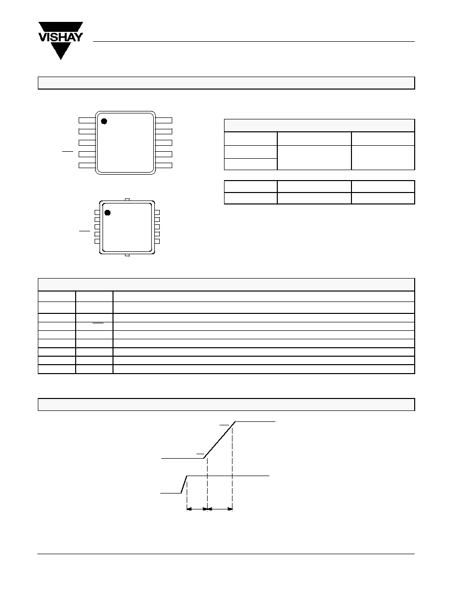
MLP33-10 or MSOP-10 Packages
APPLICATIONS
D
Cellular Phones, Cordless Phones
D
Computer Point of Use, Notebook
D
PDAs
D
Battery Powered Devices
D
MP3 Players
DESCRIPTION
The Si9177 is a dual-mode power adjustable output converter.
When it is set to PSM mode, the Si9177 operates as a
pulse-skipping-modulation controlled step-down (buck)
converter with an output voltage range of 1.2 V to 5 V. It has an
integrated MOSFET, capable of supplying 200-mA load
current with a 1.5-
m
H inductor. The output voltage is adjusted
by a resistive divider on the F
B
pin. The typical conversion
efficiency is above 90%. A logic HIGH at the BP/PSM pin puts
Si9177 in bypass mode. The main PMOS buck switch is forced
to turn on at 100% duty cycle, overriding the F
B
signal. The
voltage differential between input and output is the resistive
voltage drop on the internal 150-m
W
PMOS and the inductor.
The Si9177 delivers 800-mA load in bypass mode.
The Si9177 is available in the space saving MLP33-10 and
MSOP-10 packages. In order to satisfy the stringent ambient
temperature requirements, the Si9177 is rated to handle the
industrial temperature range of -25
_
C to 85
_
C.
TYPICAL APPLICATION CIRCUIT
V
IN
ON/OFF
ENABLE
BP/PSM
NC
SI9177
L
X
GND
F
B
REF
1
2
3
4
5
10
9
8
7
6
V
OUT
V
IN
BP/PSM
V
IN
L
X
C
IN
C
OUT
C
REF
1.5
m
H
R
1
R
2
Si9177
Vishay Siliconix
New Product
www.vishay.com
2
Document Number: 70312
S-03663--Rev. B, 07-Apr-03
ABSOLUTE MAXIMUM RATINGS (T
A
= 25_C)
V
IN
6.5 V
. . . . . . . . . . . . . . . . . . . . . . . . . . . . . . . . . . . . . . . . . . . . . . . . . . . . . . . .
BP/PSM, ENABLE, F
B,
L
X
-0.3 V to V
IN
+ 0.3 V
. . . . . . . . . . . . . . . . . . . . . . . .
Storage Temperature
-55 to 150
_
C
. . . . . . . . . . . . . . . . . . . . . . . . . . . . . . . . . .
Operating Junction Temperature
150
_
C
. . . . . . . . . . . . . . . . . . . . . . . . . . . . . .
Power Dissipation (Package)
a.
MLP33-10
b.
481 mW
. . . . . . . . . . . . . . . . . . . . . . . . . . . . . . . . . . . . . . . . . . . . . .
MSOP-10
c
915 mW
. . . . . . . . . . . . . . . . . . . . . . . . . . . . . . . . . . . . . . . . . . . . . . .
Thermal Impedance (
Q
JA
)
MLP33-10
135
_
C/W
. . . . . . . . . . . . . . . . . . . . . . . . . . . . . . . . . . . . . . . . . . . . . . .
MSOP-10
71
_
C/W
. . . . . . . . . . . . . . . . . . . . . . . . . . . . . . . . . . . . . . . . . . . . . . . . .
Notes
a.
Device mounted with all leads soldered or welded to PC board.
b.
Derate 7.4 mW/
_
C above 25
_
C.
c.
Derate 14 mW/
_
C above 25
_
C.
Stresses beyond those listed under "Absolute Maximum Ratings" may cause permanent damage to the device. These are stress ratings only, and functional operation
of the device at these or any other conditions beyond those indicated in the operational sections of the specifications is not implied. Exposure to absolute maximum rating
conditions for extended periods may affect device reliability.
RECOMMENDED OPERATING RANGE
V
IN
2.7 V to 6 V
. . . . . . . . . . . . . . . . . . . . . . . . . . . . . . . . . . . . . . . . . . . . . . . . . . .
C
IN
10
m
F
. . . . . . . . . . . . . . . . . . . . . . . . . . . . . . . . . . . . . . . . . . . . . . . . . . . . . . . .
C
OUT
10
m
F
. . . . . . . . . . . . . . . . . . . . . . . . . . . . . . . . . . . . . . . . . . . . . . . . . . . . . .
Inductor
1.5
m
H
. . . . . . . . . . . . . . . . . . . . . . . . . . . . . . . . . . . . . . . . . . . . . . . . . . .
C
REF
Open
. . . . . . . . . . . . . . . . . . . . . . . . . . . . . . . . . . . . . . . . . . . . . . . . . . . . . .
Operating Temperature Range
-25 to 85
_
C
. . . . . . . . . . . . . . . . . . . . . . . . .
SPECIFICATIONS
Test Conditions Unless Specified
40
_
C to 85
_
C V
IN
= V
DD
C
IN
= 10
m
F
Limits
Parameter
Symbol
-40
_
C to 85
_
C, V
IN
= V
DD,
, C
IN
= 10
m
F
C
OUT
= 4.7
m
F, L = 2.2
m
H, 2.6 V
v
V
IN
v
5.5 V
R
1
= 11.3 k
W
, R
2
= 20 k
W
Min
a
Typ
b
Max
a
Unit
Converter Operation
Input Voltage
V
IN
2.7
6
V
Maximum Bypass Mode Current
I
OUT
800
mA
Maximum PSM Mode Current
I
OUT
200
mA
MOSFET On-resistance
r
DS(on)
V
IN
w
3.3 V
150
300
m
W
Power Supply Rejection
PSRR
60
dB
Feedback Voltage
V
FB
I
REF
= 0
1.175
1.215
1.255
V
Feedback Voltage
V
FB
I
REF
= 0, TA = 25
_
C
1.195
1.215
1.235
V
Start-Up
Start-Up Delay Time
t
DELAY
C
REF
= 0.1
m
F, See Figure 1
5
ms
Soft Start Time
t
ss
See Figure 1
100
m
s
ENABLE, BP/PSM
Logic High
V
IH
1.5
V
Logic Low
V
IL
0.4
V
Input Current
I
IH
ENABLE, BP/PSM = V
IN
1
m
A
Input Current
I
IL
ENABLE, BP/PSM = GND
1
m
A
Protection
Under Voltage Lockout
V
UVLO
2.2
2.35
2.5
V
Under Voltage Lockout Hysteresis
V
HUVLO
0.1
V
Thermal Shutdown
T
SD
Temperature rising
165
_
C
Thermal Shutdown Hysteresis
T
HSD
V
IN
= 3.3 V
25
_
C
Supply Current
BP Mode
V
IN
= 3 3 V
75
110
PSM Mode
I
IN
V
IN
= 3.3 V
190
250
m
A
Shutdown
I
IN
V
IN
= 3.3 V, ENABLE = 0 V
1
m
A
Notes
a.
The algebraic convention whereby the most negative value is a minimum and the most positive a maximum, is used in this data sheet.
b.
Typical values are for DESIGN AID ONLY, not guaranteed or subject to production testing.
c.
Guaranteed by design and characterization, not subject to production testing.

Si9177
Vishay Siliconix
New Product
Document Number: 70312
S-03663--Rev. B, 07-Apr-03
www.vishay.com
5
DETAIL OPERATIONAL DESCRIPTION
Start-Up
When voltage is first applied to the V
IN
pin, the UVLO circuitry
prevents the internal p-channel MOSFET from turning on.
Once the V
IN
voltage exceeds the UVLO threshold of 2.4 V,
and with no other shutdown condition detected, an internal
power-on-reset timer is activated to delay the start of switching
if the BP/PSM pin is held a logic LOW level. The amount of
delay is set by the capacitor C
REF
on the REF pin and the peak
current in the inductor is limited to 600 mA. If the BP/PSM
pin
has a logic HIGH applied, then Bypass Mode soft-start is
achieved by gradually turning on the p-channel MOSFET in
40
�
s insuring that the output voltage rises smoothly.
Pulse Skipping Mode
Si9177 is designed to operate with light loads. When the
BP/PSM
pin is connected to logic LOW level, the Si9177
operates in pulse-skipping mode. PSM enhances efficiency in
light load conditions when compared to fixed frequency PWM
mode because switch conduction losses, gate charge and
switching losses are reduced. By delivering energy to the load
only when needed, the p-channel MOSFET gate capacitance
is charged and discharged less frequently and MOSFET
conduction loss is minimized thereby reducing total losses and
increasing converter efficiency. In PSM, the switching
frequency, f
SW
, increases as and decreases as the load
current increases and decreases. The typical conversion
efficiency in PSM mode is 90%.
By operating as a constant on-time converter, the Si9177
achieves PSM operation. The p-channel MOSFET switching
transistor is turned on to deliver energy to the load. The switch
remains on for the minimum on-time or until the inductor
current reaches 600 mA. If the applied on-time is sufficient to
increase the output voltage above the in-regulation set point
(F
B
pin voltage is greater than V
FB
), the p-channel MOSFET
turns off for a minimum off-time and continues to apply
constant on-time pulses to insure regulation is maintained. If
the on-time of the p-channel switch causes the output voltage
to rise above the set point, the converter turns off and remains
off until the voltage on F
B
decreases below V
FB
.
The on-time and minimum off-time are set internally to
minimize ripple voltage at the maximum load current. The
Si9177 has internal compensation reducing the number of
required components and is designed for an inductor value of
1.5
�
H and an output capacitor value of 10
�
F.
BYPASS Mode
Si9177 can also operate in BYPASS mode to handle heavy
load currents or to provide the maximum output voltage to the
load. This mode is enabled by setting the BP/PSM pin to a logic
HIGH. In this mode the IC ignores the feedback signal at the
F
B
pin, forcing the internal p-channel MOSFET to turn on
continuously. The input-to-output voltage differential is
reduced to the voltage drop across the 150-m
MOSFET and
the inductor. Si9177 can bypass 800 mA at 95% typical
efficiency or provide nearly the entire input voltage to the load.
Whenever the converter enters BYPASS mode, the p-channel
MOSFET turns on gradually within 40
�
s to reduce surge
current to the input capacitor.
Shutdown
Si9177 is designed to conserve as much battery life as
possible by decreasing current consumption during normal
operation, as well as the shutdown mode. With logic LOW level
on the ENABLE pin, the current consumption of the IC is
decreases to less than 1
�
A by shutting off all circuits. A logic
HIGH enables the controller, allowing start up as described in
the "Start-Up" section above.
Reference and Power-On-Reset Timer
The reference voltage of Si9177 is set to 1.215 V. It is internally
connected to the non-inverting input of the error amplifier. The
power on reset delay time is set by the capacitance on the REF
pin and can be determined from the following relationship:
t
PORDELAY =
4
10
4
C
REF
Output Voltage
The Si9177 is designed with an adjustable output voltage,
V
OUT
, which is set by resistors R
1
and R
2
, and the feedback
voltage, V
FB
. V
OUT
is defined according to the following
relationship:
V
OUT
+
1
)
R
1
R
2
V
FB
where V
FB
is 1.215 V.
The values of R
1
and R
2
should be kept between 5 k
and
100 k
.
Power Switches
The p-channel MOSFET switch is integrated in Si9177 for
optimum performance and minimum overall converter size.
This MOSFET is designed to minimize the gate charge loss as
well as the conduction loss. The typical on-resistance is
150 m
with a minimum input voltage of 3.3 V.