 | –≠–ª–µ–∫—Ç—Ä–æ–Ω–Ω—ã–π –∫–æ–º–ø–æ–Ω–µ–Ω—Ç: VT98001Q | –°–∫–∞—á–∞—Ç—å:  PDF PDF  ZIP ZIP |
2001-07-25 Page
1
MDST-0013-00
www.vaishali.com
Vaishali Semiconductor 747 Camden Avenue, Suite C Campbell CA 95008 Ph. 408.377.6060 Fax 408.377.6063
Applications
∑
=
Set-top boxes
∑
=
MPEG Video clock source
General Description
The Vaishali VT98001 is a single-chip, integrated multiple Phase Locked Loop (PLL) clock synthesizer. The
device uses an analog Phase Locked Loop (PLL) to accept a 27 MHz crystal input to produce multiple
outputs. Selection pins are used to provide various outputs.
Features
∑
=
24.576 MHz for Firewire IEEE1394 or video
digitizer
∑
=
24.576 MHz / 28.224 MHz for software or
hardware modem
∑
=
27 MHz buffered output clock
∑
=
6.000MHz buffered output clock
∑
=
18.432 MHz for audio processor
∑
=
2kHz standby clock
∑
=
Zero ppm synthesis error in all clocks
(except the 2 kHz standby clock)
∑
=
5V tolerant inputs
∑
=
20-pin, 150 mil SSOP (QSOP)
Advance Information
VT98001
Multifrequency Synthesizer
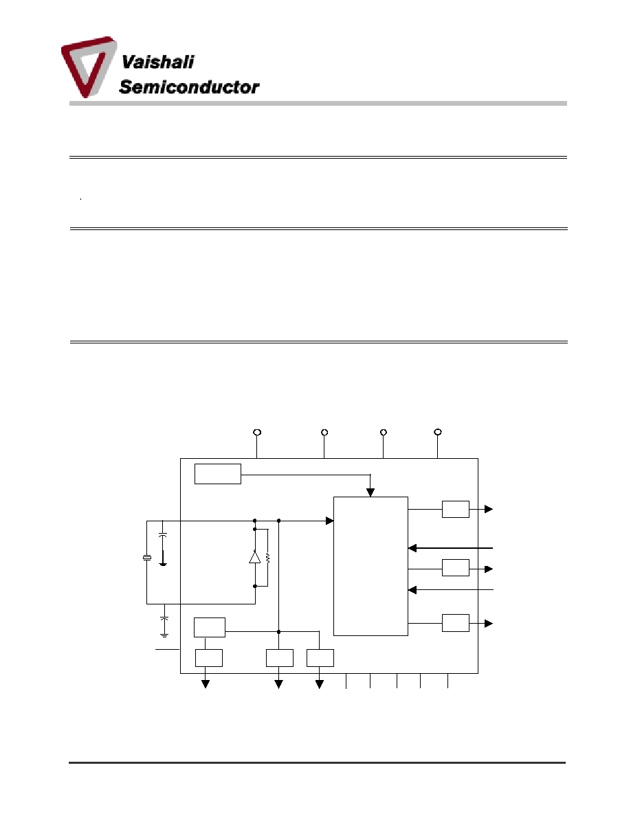
Figure 1. Functional Block Diagram
27 MHz
Crystal
24.576/
28.224 MHz
/PD
X1
GND4
27 MHz
27 MHz
GND2 GND3
2kHz
Select
24/28 MHz
X2
ROM Table
osc
VDD2
VDD3
VDD1
24.576 MHz
18.432MHz/
6.000MHz
VDD4
GND5
MODE
GND1
Buffer
Buffer
Buffer
Buffer
Buffer
Buffer
Divider
PLL
Multiplier

VT98001
Advance Information
2001-07-25 Page
2
MDST-0013-00
www.vaishali.com
Vaishali Semiconductor 747 Camden Avenue, Suite C Campbell CA 95008 Ph. 408.377.6060 Fax 408.377.6063
Figure 2. Pin Configuration
Table 1. Pin Description
Name Pin
#
Type
Description
Select 24/28 MHz
1
I(PU)
Select 24.576 MHz or 28.224 MHz output
X2
2
O
Crystal connection. Connect to a 27 MHz crystal
X1
3
I
Crystal connection. Connect to a 27 MHz crystal
VDD1
4
P
Connect to 3.3V
VDD2
5
P
Connect to VDD
GND1
6
P
Connect to ground
GND2
7
P
Connect to ground
24.576 MHz
8
O
Clock output, 24.576 MHz
MODE
9
I(PU)
Mode control. See Table 2
24.576 MHz/ 28.224MHz
10
O
Clock output, 24.576 MHz or 28.224 MHz
2 kHz
11
O
Clock output, 2 kHz
/PD
(1)
12
I(PU)
Powerdown control. When LOW, all clocks are disabled except
2kHz standby clock
18.432MHz/6.000MHz
13
O
Clock output, 18.432 MHz or 6.000 MHz
GND3
14
P
Connect to ground
GND4
15
P
Connect to ground
VDD3
16
P
Connect to VDD
VDD4
17
P
Connect to VDD
27 MHz
18,19
O
27 MHz buffered clock outputs
GND5
20
P
Connect to ground
Legend: I = Input
O = Output
P = Power supply connection
I(PU) = Input with a 250k ohm pull up
Note (1). All disabled clock outputs are tristated (high impedance).
VT98001
24.576MHz/28.224MHz
18.432MHz/6.000MHz
VDD2
GND2
X1
GND1
VDD3
24.576MHz
GND4
VDD1
27MHz
Select 24/28MHz
X2
1
2
3
4
5
6
7
8
20
19
18
17
16
15
14
13
9
10
12
11
27MHz
GND3
/PD
2kHz
MODE
GND5
VDD4

VT98001
Advance Information
2001-07-25 Page
3
MDST-0013-00
www.vaishali.com
Vaishali Semiconductor 747 Camden Avenue, Suite C Campbell CA 95008 Ph. 408.377.6060 Fax 408.377.6063
Table 2. Mode Control and Frequency Selection Table (/PD = HIGH)
(1,2)
Control
(3)
Outputs
Pin 9
Mode
Pin 1
(Select 24/28MHz).
Pin 10
(24.576 MHz / 28.224 MHz)
Pin 13
(18.43 MHz / 6 MHz)
0 0
0 1
High Impedance
18.432 MHz
1 0
24.576
MHz
1 1
28.224
MHz
6 MHz
Notes:
1.
27MHz (Pins 18 &19) and 24.576 MHz (Pin 8) are active, unless /PD = LOW
2. 2 kHz standby clock is always active, independent of /PD logic state
3. 0 = Low, 1 = HIGH
Table 3. Recommended Crystal Specification
Frequency accuracy is directly proportional to the capacitive load (CL) of the crystal.
Parameter Definition
Min
Typ
Max
Units
Frequency at CL, FL
Defines the series resonant
frequency at CL
27.000
MHz
Total accuracy: includes initial
accuracy @ 25∫C, aging, and
temperature drift (25∫C to 70∫C)
Maximum deviation from
nominal frequency @ 25∫C,
taking in to account aging,
and temperature drift
40
ppm
Load Capacitance CL
Capacitive load for nominal
frequency FL
20
pf
C1
Motional capacitance of the
crystal
TBD
pf
C0
Shunt capacitance of the
crystal
7
pf
ESR Equivalent
Series
Resistance of the crystal
40
ohms
Table 4. Operating Conditions
Parameter Conditions
Min
Typ
Max
Units
Power Supply Voltage, V
DD
3.0 3.3
3.6
V
Input High Voltage, V
IH
2.0
V
DD
V
Input Low Voltage, V
IL
0.8
V
Operating Temperature,T
A
0 25
70
∫C
Table 5. Electrical Characteristics
Parameter Symbol
Min
Typ
Max
Units
Output voltage high I
OH
= -8 mA
VOH
2.7
V
Output voltage low I
OL
= 8 mA
VOL
0.4
V
Maximum input capacitance (X1,X2)
Cin
3
pF
Power consumption (operating)
I
dd1
mA
Power consumption (powerdown)
I
dd2
mA

VT98001
Advance Information
2001-07-25 Page
4
MDST-0013-00
www.vaishali.com
Vaishali Semiconductor 747 Camden Avenue, Suite C Campbell CA 95008 Ph. 408.377.6060 Fax 408.377.6063
Table 6. Phase Noise Requirements (Crystal phase noise must be less than
-
130 dBc/Hz @ 10kHz)
Parameter Symbol
Min
Typ
Max
Units
27 MHz
-120
dBc/Hz @ 10 kHz
24.576 MHz
-100
dBc/Hz @ 10 kHz
24.576/28.224 MHz
-100
dBc/Hz @ 10 kHz
18.432/6.000 MHz
-100
dBc/Hz @ 10 kHz
Table 7. Output Accuracies (Excluding crystal accuracy)
Parameter Symbol
Min
Typ
Max
Units
24.576/28.224 MHz
0
ppm
2kHz
50
%
18.432/6.000 MHz
0
ppm
27 MHz
0
ppm
Table 8 AC Characteristics
All @Cload = 20 pF, VDD = 3.0V to 3.6V
Parameter Symbol
Min
Typ
Max
Units
Duty Cycle @ V
DD
/2
45/55 %
Rise time ( measured between 0.8V
and 2.0V)
Tr 1
2.5
ns
Fall time ( measured between 0.8V
and 2.0V)
Tf 1
2.5
ns
PLL lock time
Tlock
ms
Time to clock outputs after VDD is
available
Tst
50
ms
Ordering Information
Part Number
Marking
Shipping/Packaging
No. of Pins
Package
Temperature
VT98001Q VT98001Q
Tubes
20
QSOP
0
∞
C to +70
∞
C
VT98001QX
VT98001Q
Tape & Reel
20
QSOP
0
∞
C to +70
∞
C