Vectron International 267 Lowell Road, Hudson, NH 03051 Tel:1-88-VECTRON-1 e-mail: vectron@vectron.com
CD-700
Complete VCXO Based Phase Lock Loop
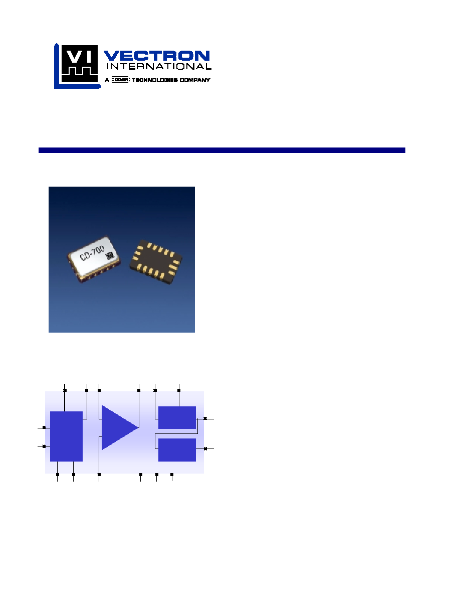
Figure 1. CD-700 Block Diagram
Features
∑
5 x 7.5 x 2 mm, smallest VCXO PLL available
∑
Output Frequencies to 65.536 MHz
∑
5.0 or 3.3 Vdc operation
∑
Tri-State Output
∑
Loss of Signal Alarm
∑
VCXO with CMOS outputs
∑
0/70 or ≠40/85
∞
C temperature range
∑
Hermetically sealed ceramic SMD package
Applications
∑
Frequency Translation
∑
Clock Smoothing, Clock Switching
∑
NRZ Clock recovery
∑
DSLAM, ADM, ATM, Aggregation, Optical
Switching/Routing, Base Station
∑
Low jitter PLL's
Description
The VI CD-700 is a user-configurable crystal
based PLL integrated circuit. It includes a digital
phase detector, op-amp, VCXO and additional
integrated functions for use in digital
synchronization applications. Loop filter software
is available as well SPICE models for circuit
simulation.
DATAIN
(5)
CLKIN
(6)
VDD
(14)
HIZ
(12)
GND
(7)
OUT2
(11)
RCLK
(9)
RDATA
(10)
OPP
(15)
LOS
(8)
PHO
(3)
OPN
(2)
OPOUT
(1)
VC
(16)
LOSIN
(4)
OP-Amp
VCXO
OUT1
(13)
Optional
2
n
Divider
Phase
Detector
and LOS

CD-700, VCXO Based PLL
Vectron International 267 Lowell Road, Hudson, NH 03051 Tel:1-88-VECTRON-1 e-mail: vectron@vectron.com
Performance Characteristics
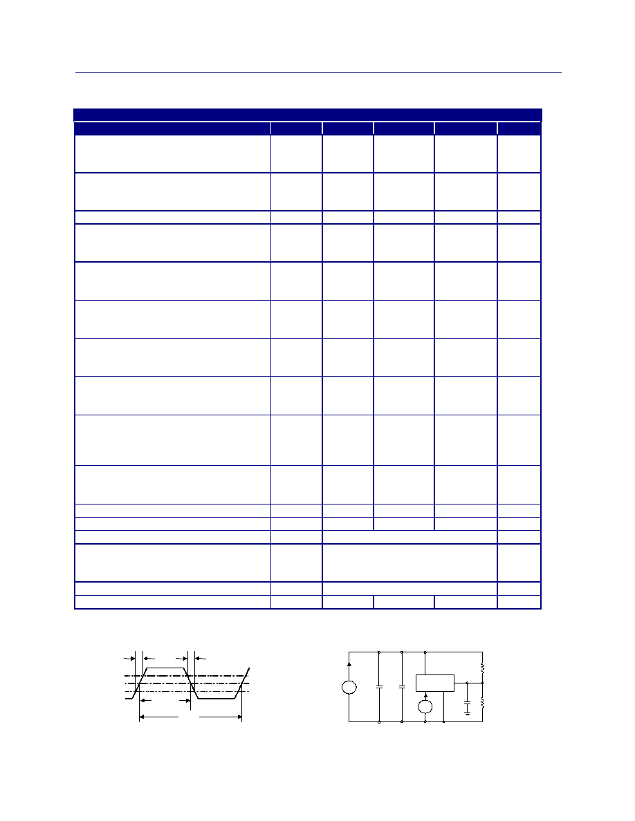
Table 1. Electrical Performance
Parameter
Symbol
Min
Typical
Maximum
Units
Output Frequency (ordering option)
OUT1, 5.0 V option
OUT1, 3.3 V option
12.000
12.000
65.536
51.840
MHz
MHz
Supply Voltage
1
+5.0
+3.3
V
DD
4.5
2.97
5.0
3.3
5.5
3.63
V
V
Supply Current
I
DD
63
mA
Output Logic Levels
Output Logic High
2
Output Logic Low
2
V
OH
V
OL
2.5
0.5
V
V
Output Transition Times
Rise Time
2
Fall Time
2
t
R
t
F
5
5
ns
ns
Input Logic Levels
Output Logic High
2
Output Logic Low
2
V
IH
V
IL
2.0
0.5
V
V
Loss of Signal Indication
Output Logic High
2
Output Logic Low
2
V
OH
V
OL
2.5
0.5
V
V
Nominal Frequency on Loss of Signal
Output 1
Output 2
±
75
±
75
ppm
ppm
Symmetry or Duty Cycle
3
Out 1
Out 2
RCLK
SYM1
SYM2
RCLK
40/60
45/55
40/60
%
%
%
Absolute Pull Range (ordering option)
over operating temperature, aging, and
power supply variations
APR
±
50
±
80
±
100
ppm
Test Conditions for APR (+5.0 V option)
V
C
0.5
4.5
V
Test Conditions for APR (+3.3 V option)
V
C
0.3
3.0
V
Gain Transfer
Positive
Phase Detector Gain
+5V option
+3.3V option
0.53
0.35
rad/V
rad/V
Operating temperature (ordering option)
0/70 or ≠40/85
∞
C
Control Voltage Leakage Current
I
VCXO
±
1
uA
1. A 0.01uF and 0.1uF parallel capacitor should be located as close to pin 14 as possible (and grounded).
2. Figure 2 defines these parameters. Figure 3 illustrates the equivalent five gate TTL load and operating conditions under which
these parameters are tested and specified. Loads greater than 15 pF will adversely effect rise/fall time as well as symmetry.
3. Symmetry is defined as (ON TIME/PERIOD with Vs=1.4 V for both 5.0 V and 3.3 V operation.
Figure 2. Output Waveform
Figure 3. OUT1, OUT2, RCLK, RDATA
Test Conditions (25
±
±
±
±
5∞C)
80
%
1.4V
20
%
t
F
t
R
Period
On Time
+
-
+
-
I
C
V
C
13
.
1
µ
F
.01
µ
F
15pF
14
16
I
DD
650
V
DD
1.8k
7

CD-700, VCXO Based PLL
Vectron International
∑
267 Lowell Road, Hudson, NH 03051
∑
Tel: 1-88-VECTRON-1
∑
http://www.vectron.com
Absolute Maximum Ratings
Stresses in excess of the absolute maximum ratings can permanently damage the device. Functional
operation is not implied at these or any other conditions in excess of conditions represented in the
operational sections of this data sheet. Exposure to absolute maximum ratings for extended periods may
adversely affect device reliability.
Table 2. Absolute Maximum Ratings
Parameter
Symbol
Ratings
Unit
Power Supply
V
DD
7
Vdc
Storage Temperature
Tstorage
-55/125
∞
C
Clock and Data Input Range
CLKIN, DATAIN
Gnd-0.5 to V
DD
+0.5
V
Reliability
The CD-700 is capable of meeting the the following qualification tests.
Table 3. Environmental Compliance
Parameter
Conditions
Mechanical Shock
MIL-STD-883, Method 2002
Mechanical Vibration
MIL-STD-883, Method 2007
Solderability
MIL-STD-883, Method 2003
Gross and Fine Leak
MIL-STD-883, Method 1014, 100% Tested
Resistance to Solvents
MIL-STD-883, Method 2016
Handling Precautions
Although ESD protection circuitry has been designed into the the CD-700, proper precautions should be
taken when handling and mounting. VI employs a Human Body Model (HBM) and a Charged Device
Model (CDM) for ESD susceptibility testing and design protection evaluation. ESD thresholds are
dependent on the circuit parameters used to define the model.
Table 4. Predicted ESD Ratings
Model
Minimum
Conditions
Human Body Model
1500 V
MIL-STD 883, Method 3015
Charged Device Model
1000 V
JESD 22-C101

CD-700, VCXO Based PLL
Vectron International
∑
267 Lowell Road, Hudson, NH 03051
∑
Tel: 1-88-VECTRON-1
∑
http://www.vectron.com
CD-700 Theory of Operation
Phase Detector
The phase detector has two buffered inputs (DATAIN and CLKIN) which are designed to switch at
1.4 volts. DATAIN is designed to accept an NRZ data stream but may also be used for clock signals which
have a 50% duty cycle. CLKIN is connected to OUT1 or OUT2, or a divided version of one of these
outputs. CLKIN and DATAIN and are protected by ESD diodes and should not exceed the power supply
voltage or ground by more than a few hundred millivolts.
The phase detector is basically a latched flip flop/exclusive-or gate/differential amplifier filter design to
produce a DC signal proportional to the phase between the CLKIN and DATAIN signals (see Figure 4 for
a block diagram and Figure 5 for an open loop transfer curve). This will simplify the PLL design as the
designer does not have to filter narrow pulse signals to a DC level. Under locked conditions the rising
edge of CLKIN will be centered in the middle of the DATAIN signal (see Figure 6).
The phase detector gain is 0.53V/rad x data density for 5volt operation and 0.35V/rad x data density for
3.3 volt operation. Data density is equal to 1.0 for clock signals and is system dependent on coding and
design for NRZ signals, but 0.25 could be used as a starting point for data density.
The phase detector output is a DC signal for DATAIN frequencies greater than 1 MHz but produces
significant ripple when inputs are less than 200 kHz. Additional filtering is required for lower input
frequencies applications such as 8kHz (see Figures 8 and 9 as examples).
Under closed loop conditions the active filter has a blocking capacitor which provides a very high DC gain,
so under normal locked conditions and input frequencies >1 MHz, PHO will be about V
DD
/2 and will not
vary significantly with changes in input frequency (within lock range). The control voltage (pin 16) will vary
according to the input frequency offset, but PHO will remain relatively constant.
D
Q
1
Q
2
D
Gain = 2 / 3
Gain = V
DD
/ 2
30 k
20 k
PHO
(pin 3)
Clock In
(pin 6)
Data In
(pin 5)
Figure 4. Simplified Phase Detector Block Diagram

CD-700, VCXO Based PLL
Vectron International
∑
267 Lowell Road, Hudson, NH 03051
∑
Tel: 1-88-VECTRON-1
∑
http://www.vectron.com
V
DD
0V
0
+
-
Relative
Phase (
e
)
V
DD
/2
V
d
Gain Slope = V
DD
/ 2
Figure 5. Open Loop Phase Detector Transfer Curve
Recovered Clock and Data Alignment Outputs
The CD-700 is designed to recover an embedded clock from an NRZ data signal and retime it with a data
pattern. In this application, the VCXO frequency is exactly the same frequency as the NRZ data rate and
the outputs are taken off Pin 9 (RCLK), and Pin 10 (RDATA). Under locked conditions, the falling edge of
RCLK is centered in the RDATA pattern. Also, there is a 1.5 clock cycle delay between DATAIN and
RDATA. Figure 6 shows the relationship between the DATAIN, CLKIN, RDATA and RCLK.
Figure 6. Clock and Data Timing Relationships for the NRZ data
Other RZ encoding schemes such as Manchester or AMI can be accomodated by using a CD-700 at twice
the baud rate.
Loss of Signal, LOS and LOSIN
The LOS circuit provides an output alarm flag when the DATAIN input signal is lost. The LOS output is
normally a logic low and is set to a logic high after 256 consecutive clock periods on CLKIN with no
detected DATAIN transitions. This signal can be used to either flag external alarm circuits and/or drive the
CD-700's LOSIN input. When LOSIN is set to a logic high, the VCXO control voltage (pin 16) is switched
to an internal voltage which sets OUT1 and OUT2 to center frequency +/-75ppm. Also, LOS automatically
closes the op amp feedback which means the op-amp is a unity gain buffer and will produce a DC voltage
equal to the +op amp voltage (pin 15), usually V
DD
/2.
Data1
Clock In
CLKIN
Data In
DATAIN
Recovered Data
RDATA
Recovered Clock
RCLK

CD-700, VCXO Based PLL
Vectron International
∑
267 Lowell Road, Hudson, NH 03051
∑
Tel: 1-88-VECTRON-1
∑
http://www.vectron.com
VCXO and Absolute Pull Range (APR) Specification
The CD-700's VCXO is a varactor tuned crystal oscillator, which produces an output frequency
proportional to the control voltage (pin 16). The frequency deviation of the CD-700 VCXO is specified in
terms of Absolute Pull Range (APR). APR provides the user with a guaranteed specification for minimum
available frequency deviation over all operating conditions. Operating conditions include power supply
variation, operating temperature range, and differences in output loading and changes due to aging.
A CD-700 VCXO with an APR of +/-50 ppm will track a +/-50 ppm reference source over all
operating conditions. The fourth character of the product code in Table 7 specifies absolute Pull
Range (APR). Please see Vectron's web site (www.vectron.com) for the APR Application Note.
APR is tested at 0.5 and 4.5 volts for the 5.0 volt option and 0.3 and 3.0 volts for the 3.3 volt option.
VCXO Aging
Quartz oscillators typically exhibit a part per million shift in output frequency during aging. The major
factors, which lead to this shift, are changes in the mechanical stress on the crystal and mass-loading on
the crystal.
As the oscillator ages, relaxation of the crystal mounting stress or transfer of environmental stress through
the package to the crystal mounting arrangement can lead to frequency variations. VI has minimized these
two effects through the use of a miniature AT-cut strip resonator crystal which allows a superior mounting
arrangement. This results in minimal relaxation and almost negligible environmental stress transfer.
VI has eliminated the impact of mass loading by ensuring hermetic integrity and minimizing out-gassing by
limiting the number of internal components through the use of ASIC technology. Mass-loading on the
crystal generally results in a frequency decrease and is typically due to out-gassing of material within a
hermetic package or from contamination by external material in a non-hermetic package.
Under normal operating conditions the CD-700 will typically exhibit 2 ppm aging in the first year of
operation. The device will then typically exhibit 1 ppm aging the following year with a logarithmic decline
each year thereafter.
Frequency Divider Feature
The lowest available VCXO OUT1 frequency is 12.000 MHz. To achieve lower frequencies, OUT1 is
divided by a 2
n
counter (n = 1 to 8) and is the OUT2 frequency. The divider values (2, 4, 8, 16, 32, 64, 128
and 256) are set at the factory, so it is user selectable upon ordering only. In addition, a disabled OUT2
option is also available. To achieve 1.544 MHz, a CD-700 with OUT1 frequency equal to 24.704 MHz
and a divider value equal to 16 would be used. Additional external divider circuits can be used to further
lower or change the frequency.

CD-700, VCXO Based PLL
Vectron International
∑
267 Lowell Road, Hudson, NH 03051
∑
Tel: 1-88-VECTRON-1
∑
http://www.vectron.com
Loop Filter
A PLL is a feedback system which forces the output frequency to lock in both phase and frequency to the
input frequency. While there will be some phase error, theory states there is no frequency error. The loop
filter design will dictate many key parameters such as jitter reduction, stability, lock range and acquisition
time. Be advised that many textbook equations describing loop dynamics, such as capture range are
based on ideal systems. Such equations may not be accurate for real systems due to nonlinearities, DC
offsets, noise and do not take into account the limited VCXO bandwidth. This section deals with some real
world design examples. Also, there is loop filter software on the Vectron web site, plus a full staff of
experienced applications engineers who are eager to assist in this process. Common CD-700 PLL
applications are shown in Figures 8, 9 (frequency translation), Figure 10 (clock recovery) and
Figure 11 (clock smoothing).
Of primary concern to the designer is selecting a loop filter that insures lock-in, stability and provides
adequate filtering of the input signal. For low input frequencies, a good starting point for the loop filter
bandwidth is
10 Hz (typical).
An example would be translating an 8 kHz signal to 44.736 MHz.
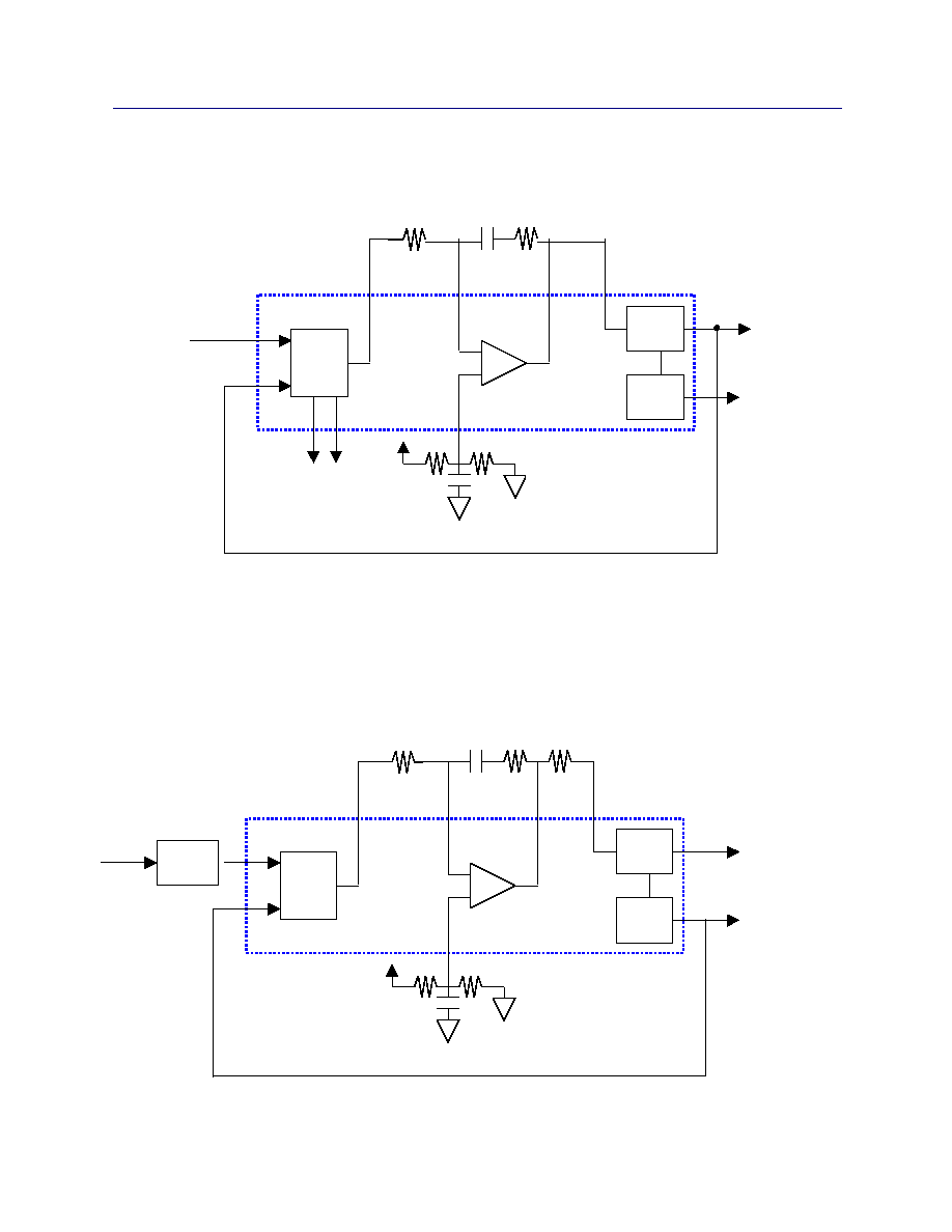
Figures 8 and 9 show 8kHz to 44.736 MHz and 8kHz to 19.440 MHz frequency translation designs.
For high input frequencies, a good starting point for the loop filter bandwidth is 100 ppm times the input
frequency.
It's fairly easy to set a low loop bandwidth for large frequency translations such as 8kHz to 44.736MHz,
but becomes more difficult for clock smoothing applications such as 19.440 MHz input and 19.440MHz
output. In this example, 100ppm * 19.440MHz is approximately 2kHz and this loop filter bandwidth may
be too high to adequately reject jitter. A good way to resolve this is to lower the DATAIN frequency such
as dividing the input frequency down. The loop filter bandwidth becomes lower since 100ppm * DATAIN is
lowered. Figure 11 shows an example for clock smoothing on a relatively high input frequency signal and
maintaining a wide lock range.
There is no known accurate formula for calculating acquisition time and so the best way to provide realisitc
figures is to measure the lock time for a CD-700. By measuring the control voltage settling time, acquisiton
time was measured in the range of 3-5 seconds for applications such as 8kHz to 34.368 MHz frequency
translation which is similar to the application in Figures 8 and 9, to sub 10 milliseconds for NRZ data
patterns such as Figure 10. It may be tempting to reduce the damping factor to 0.7 or 1.0 in order to
improve acquisition time; but, it degrades stability and will not signifigantly improve acquisition time. A
damping factor of 4 is fairly conservative and allows for excellent stability.
Some general quidelines for selecting the loop filter elements include: Values should be less than
1Megohm and at least 10kohm between the PHO and OPN, the capacitor should be low leakage and a
polarized capacitor is acceptable, the R/C's should be located physically close to the CD-700 .The loop
filter software available on the web site was written for 5 volt operation. A simple way to calculate values
for 3.3 volt operation is to multiply the data density by 0.66 (3.3V / 5V).
SPICE models are another design aid. In most cases a new PLL CD-700 design is calculated by using the
software and verified with SPICE models. The simple active
model is shown in Figure 7.
Loop filter values can be modified to suit the system requirements and application. There are many
excellent references on designing PLL's, such as "Phase-Locked Loops, Theory, Design and
Applications", by Roland E Best (McGraw-Hill).

CD-700, VCXO Based PLL
Vectron International
∑
267 Lowell Road, Hudson, NH 03051
∑
Tel: 1-88-VECTRON-1
∑
http://www.vectron.com
Figure 7. SPICE Model
*****CD-700 ac Loop model
vi 1 0 ac 1
ri 1 0 1k
*****Phase Detector
e1 2 0 1 0 1 (for closed loop response use: e1 2 0 1 12 1)
r2 2 3 30k
c1 3 0 60p
*****Phase Detector Gain=0.53 x Data Density (Data Density = 1 for clocks) for 5 volt
operation and = 0.35 x Data Density for 3.3 volt operation
e2 4 0 3 0 .35
*****Loop filter
r1 4 5 60k
c2 5 0 10p
rf 5 6 90k
cf 6 7 1.0u
e3 7 0 5 0 ≠10000
***** VCXO, Input Bandwidth=50kHz
r5 7 8 160k
c4 8 0 20p
*****VCXO Gain x 2
(Example: 19.440 MHz x 100 ppm x 2 x
)
e4 9 0 8 0 12214
*****1/S model
r6 9 10 1000
c5 10 11 0.001u
e5 11 0 10 0 ≠1e
6
****Divide by n
e6 12 0 11 0 1
r7 12 0 1k
The bold numbers are user selectable R and C values that will vary depending
on the application (see Figure 11).
Vi Ri E1 R2 C1 E2 R1 C2 Rf Cf E3 R5 C4 E4 R6 C5 E5 E6 R7
1 2 3 4 5 6 7 8 9 10 11 12

CD-700, VCXO Based PLL
Vectron International
∑
267 Lowell Road, Hudson, NH 03051
∑
Tel: 1-88-VECTRON-1
∑
http://www.vectron.com
Layout Considerations
To achieve stable, low noise performance good analog layout techniques should be incorporated and a
partial list is shown below.
The CD-700 should be treated more like an analog device and the power supply must be well decoupled
with a good quality RF 0.01 uF capacitor in parallel with a 0.1 uF capacitor, located as close to pin 14 as
possible and connected to ground. In some cases, a
filter such as a large capacitor (10uF) to ground, a
series ferrite bead or inductor with 0.01 uF and 100 pF capacitor to ground to decouple the device supply.
The traces for the OUT1, OUT2, RCLK and RDATA ouputs should be kept as short as possible. It is
common practice to use a series resistor ( 50 to 100 ohms ) in order to reduce reflections if these traces
are more than a couple of inches long. Also OUT1, OUT2, RCLK and RDATA should not be routed
directly underneath the device.
The op-amp loop filter components should be kept as close to the device as possible and the feedback
capacitor should be located close to the op-amp input terminal. The loop filter capacitor(s) should be low
leakage (polarized capacitors are allowed).
Unused outputs should be left floating and it is not required to load or terminate them (such as an ECL or
PECL output). Loading unused outputs will only increase current consumption.

CD-700, VCXO Based PLL
Vectron International
∑
267 Lowell Road, Hudson, NH 03051
∑
Tel: 1-88-VECTRON-1
∑
http://www.vectron.com
Figure 8. 8kHz to 44.736 MHz Frequency Translation
Figure 9. 8kHz to 19.44MHz Frequency Translation
8 kHz (pin 5)
pin 13
pin 1
pin 15
pin 16
pin 2
pin 3
20k 0.01uF 20k 2.2uF 330k 20k 0.1uF
10k , 2.2uF
10k
˜
1215
16kHz (pin 6)
CD-700
19.440MHz
44.736 MHz
8 kHz (pin 5)
pin 1
pin 15
pin 16
pin 2
pin 3
10k 0.01uF 10k 2.2uF 330k 20k 0.1uF
10k , 2.2uF
10k
˜
2796
16kHz (pin 6)
CD-700
pin 13
VCXO
VCXO
˜
˜
3.3 V
3.3 V

CD-700, VCXO Based PLL
Vectron International
∑
267 Lowell Road, Hudson, NH 03051
∑
Tel: 1-88-VECTRON-1
∑
http://www.vectron.com
Figure 10. 40.000 MHz NRZ Clock Recovery
Figure 11. 19.440 MHz Clock Smoothing
40.000 Mb/s (pin 5)
pin 13
40.000 MHz
pin 16
pin 1
pin 2
pin 3
55k 0.1uF 55k
5.0 V
10k, 2.2uF
10k
(pin 6)
CD-700
19.440 MHz
19.440 MHz (pin 5)
2.430 MHz
pin 11
pin 13
pin 6
60k 1.0uF 90k 10k
10k, 2.2uF , 10k
CD-700
pin 15
pin16
pin 1
pin 2
pin 3
˜
16
pin 15
VCXO
˜
VCXO
˜
8
3.3 V

CD-700, VCXO Based PLL
Vectron International
∑
267 Lowell Road, Hudson, NH 03051
∑
Tel: 1-88-VECTRON-1
∑
http://www.vectron.com
Figure 12. Suggested IR profile
Tape Dimensions (mm)
Reel Dimensions (mm)
A
B
C
D
E
F
G
H
I
J
K
L
#/
reel
16
7.5
1.5
4
8
1.5
20.2
13
50
6
16.4
178
500
Figure 13. Tape and Reel
TIME(s)
TEM
P
ER
A
T
U
R
E(
∞C
)
A
E
C
D
B
G
F
J
L
I
K
H

CD-700, VCXO Based PLL
Vectron International
∑
267 Lowell Road, Hudson, NH 03051
∑
Tel: 1-88-VECTRON-1
∑
http://www.vectron.com
1
9
5
6
8
13
14
16
CLAFGAB
FREQUENCY
VI YWW
2 3 4
7
10
11
12
15
Figure 14. Outline Diagram
Table 5. Pin Function
Pin
Symbol
Function
1
OPOUT
Op-Amp Output
2
OPN
Op-Amp Negative Input
3
PHO
Phase detector Output
4
LOSIN
INPUT (Used with LOS)
Logic 0, VCXO control voltage is enabled.
Logic 1, VCXO control voltage (pin 16) is disabled and OUT1 and OUT2 are within +/-75 ppm
of center frequency
Has Internal pull-down resistor
5
DATAIN
Phase detector Input signal (TTL switching thresholds)
6
CLKIN
Phase detector Clock signal (TTL switching thresholds)
7
GND
Cover and Electrical Ground
8
LOS
OUTPUT (Used with LOSIN)
Logic 1 if there are no transitions detected at DATAIN after 256 clock cycles at CLKIN. As soon
as a transition occurs at DATAIN, LOS is set to a logic low.
Logic 0 = Input frequency detected
9
RCLK
Recovered Clock
10
RDATA
Recovered Data
11
OUT2
Divided-down VCXO Output, or Disabled
12
HIZ
INPUT
Logic 0, OUT1, OUT2, RCLK, RDATA are set to a high impedance state.
Logic 1, OUT1, OUT2, RCLK, RDATA are active.
Has Internal pull-up resistor
13
OUT1
VCXO Output
14
V
DD
Power Supply Voltage (3.3 V
±
10% or 5.0 V
±
10%)
15
OPP
Op-Amp Positive Input
16
V
C
VCXO Control Voltage

CD-700, VCXO Based PLL
Vectron International
∑
267 Lowell Road, Hudson, NH 03051
∑
Tel: 1-88-VECTRON-1
∑
http://www.vectron.com
Ordering Information
Table 6. Standard OUT1 Frequencies (MHz)
12.000
12.288
12.352
13.000
16.000
16.384
19.440
20.000
20.480
24.576
24.704
25.000
27.000
28.704
30.000
30.720
32.000
32.768
34.368
35.328
38.880
39.3216
40.000
40.960
44.736
49.152
51.840
54.000
60.000
61.440
62.208
62.500
65.536
Other frequencies may be available upon request
Table 7. Part Number Ordering Information
CD-700- L A C - G A B - XX.XXX
(frequency in MHz)
Power Supply
Duty Cycle
K: 5.0 Vdc
B=40/60% (Out 1)
L: 3.3 Vdc
OUT2 (DIVIDER)
Output
A: Divide by 2
A: CMOS
B: Divide by 4
C: Divide by 8
Temperature Range
D: Divide by 16
C: 0 to 70
∞
C
E: Divide by 32
F: -40 to 85
∞
C
F: Divide by 64
G: Divide by 128
Absolute Pull Range
H: Divide by 256
G:
±
50 ppm
K: Disable
N:
±
80 ppm
H:
±
100 ppm
www.vectron.com
Vectron International reserves the right to make changes to the product(s) and/or information contained herein without notice. No liability is assumed as
a result of their use or application. No rights under any patent accompany the sale of any such product(s) or information.
CD-700.DOC (REVISION DATE
:
10/31/01,08/20/02)
For Additional Information, Please Contact:
USA: Vectron International
∑
267 Lowell Road, Hudson, NH 03051
∑
Tel: 1-88-VECTRON-1
∑
Fax: 1-888-FAX-VECTRON
EUROPE:
Tel: 49 (0) 3328 4784 17
∑
Fax: 49 (0) 3328 4784 30
ASIA:
Tel: +86 21 28909740 / 41 / 42 ∑ Fax: +86 21 28909240 / 28909999
