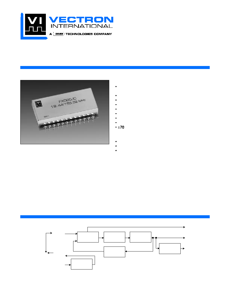
Preliminary Data Sheet
FX060
Frequency Translator
Features
19.44 MHz and 155.52 MHz Clock Outputs
Locked to an 8 kHz or 1.544 MHz Input Clock
Commercial or Industrial Temperature Range
Surface Mount Option Available
Single 5.0 Vdc Supply
AC/HCMOS Compatible Inputs and Outputs
Lock Detect Circuit
<10 ps rms Output Jitter at 19.44 MHz
19 ps rms Typical Output Jitter at 155.52 MHz
ppm Input Frequency Tolerance
Applications
Clock Frequency Translation
SONET/SDH/ATM
Clock Distribution
Description
Vectron s FX060 frequency translator is a low noise,
narrow band PLL that generates 155.52 MHz and
19.44 MHz output clocks locked to an input 8 kHz or
1.544 MHz reference clock. The 19.44 MHz clock is
generated by a low noise VCXO. The 155.52 MHz
signal is a multiplied representation of the 19.44 MHz
output.
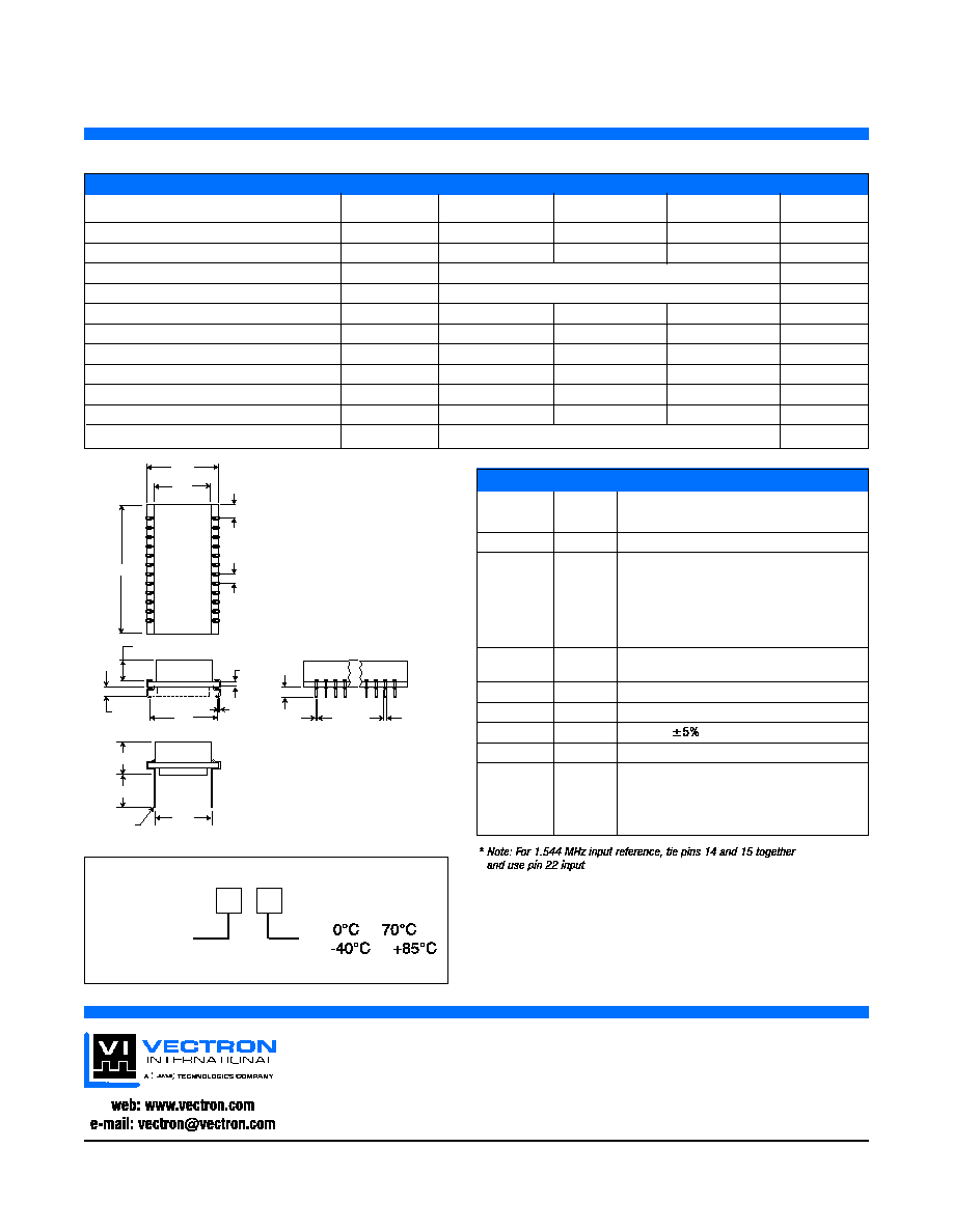
Block Diagram
Phase
Detector
Frequency
Divider
Loop
Filter
19.44 MHz
VCXO
Frequency
Multiplier
Lock
Detect
19.44 MHz
Output
155.52 MHz
Output
8 kHz
Input
User
connection
when
1.544 MHz
input is
used
8 kHz
Output
1.544 MHz
Input
Frequency
Divider
*This Bulletin is provided for informational purposes to enable early engineering discussions.
It should not be assumed that the product described in this document is qualified or available for manufacture.
FX060 Frequency Translator
Vectron International reserves the right to make changes to the product(s) and/or information contained herein without notice.
No liability is assumed as a result of their use or application. No rights under any patent accompany the sale of any such product(s) or information.
Printed in USA 2/99
1.38
12
13
.73
.225
.007
.051
.004
.019
.036
.116
9
24
.600
.28 MAX
.010X.024
.39
.105
.MAX
Thru-Hole Option
J-Lead Option
24
1
.100
.140
.80
.600
TYP.
TYP.
SEE NOTE 2
1. Pin numbers are for ref only.
They do not appear on the unit.
2. Components are mounted below
in this area and not to exceed dim. shown.
Table 1. Performance Characteristics
Parameter
Symbol
Minimum
Typical
Maximum
Units
Supply Voltage
V
DD
4.75
5.0
5.25
V
Supply Current
I
DD
-
60
100
mA
Input Signal
CLKIN
AC/HCMOS
-
Output Load
CLKOUT
AC/HCMOS
-
Output Symmetry
DC
45
50
55
%
19.44 MHz Output Clock Edge Jitter
J
19.44
-
-
10
ps rms
155.52 MHz Output Clock Jitter
J
155.52
-
19
-
ps rms
Rise/Fall Time of 19.44 MHz Output
T
R/F
-
-
7
ns
Rise/Fall Time of 155.52 MHz Output
T
R/F
-
-
2
ns
Input Frequency Tolerance
-
-70
-
+70
ppm
Output Frequency Stability
Tracks reference stability when locked
Performance Characteristics
Outline Drawing
Dimensions are in inches
Table 2. Pin Function
Pin
Symbol
Function
1
OUT19
19.44 MHz Clock Output
3
OUT155
155.52 MHz Clock Output
10
L
OCK
Lock Detect Output.
Lock indicated by Logic High. When
not locked output toggles at a rate
proportional to the phase difference
between the input clock and the
internal crystal oscillator
.
14 OUT8
8
kHz
Clock
Output
from
1.544
MHz
reference clock
15
IN8
8 kHz Reference Clock Input.
22
IN1.5
1.544 MHz
R
eference Clock Input*
24
VDD
5 Vdc
Supply
2,6,12,19
GND
Case Ground
4,5,7,8,9,
11,13,16,
N/C
No User Connection
17,18,20,
21, 23
Handing Precautions
Although protection circuitry has been designed into this
device, proper precautions should be taken to avoid exposure
to electrostatic discharge (ESD) during handling and mounting.
How to Order
FX060
J = J lead
T = Thru Hole
C =
to
L =
to
USA: Vectron International 267 Lowell Road, Hudson, NH 03051 . . . . . . . . . . . . . Tel: 1-88-VECTRON-1 Fax: 1-888-FAX-VECTRON
EUROPE: . . . . . . . . . . . . . . . . . . . . . . . . . . . . . . . . . . . . . . . . . . . . . . . . . . . . . . . . . . . Tel: 49 (0) 3328 4784 17 Fax: 49 (0) 3328 4784
30ASIA: . . . . . . . . . . . . . . . . . . . . . . . . . . . . . . . . . . . . . . . . . . . . Tel: +86 21 28909740 / 41 / 42 Fax: +86 21 28909240 / 28909999