
Product Data Sheet
VC-800
Voltage Controlled Crystal Oscillator
Features
∑ Worlds Smallest VCXO, 5.0 x 3.2 x 1.5 mm
∑ High Frequencies to 51.84 MHz
∑ 5 or 3.3 V operation
∑ Linearity
10%
∑ Tri-State Output
∑ Low jitter < 6ps rms
∑ VCXO with CMOS outputs
∑ 0/70 or ≠40/85∞C temperature range
∑ Hermetically sealed ceramic SMD package
Applications
∑ SONET/SDH
∑ DWDM
∑ xDSL/PCMCIA cards
∑ Digital Video
Description
Vectron's VC-800 Voltage Controlled Crystal Oscillator
(VCXO) is a quartz stabilized square wave generator
with a CMOS output and is tested at CMOS and TTL
(5 volt operation) logic levels.
The VC-800 is the smallest available VCXO making it
ideally suitable for PCMCIA applications as well as any
other where size is limited but performance is required.

VC-800 Voltage Controlled Crystal Oscillator
Performance Characteristics
Electrical Performance
Vectron International ∑
267 Lowell Road, Hudson, NH 03051
∑ Tel: 1-88-VECTRON-1 ∑ Fax: 1-888-FAX-VECTRON
2
.
Figure 1. Output Waveform
Conditions (25±5∞C)
Figure 2. Typical Output Test
1. A 0.01uF and a 0.1uF capacitor should be located as close to the supply as possible (to ground) is recommended.
2. Figure 1 defines these parameters. Figure 2 illustrates the equivalent five gate TTL load and operating conditions under
which these parameters are tested and specified.
3. Symmetry is defined as (ON TIME/PERIOD with Vs = 1.4 V for TTL and Vs=2.5 V for CMOS, 5 volt operation, and
Vs=1.65V for 3.3 Volt operation.
4. Load Capacitor will depend on frequency.
Frequency
f
O
1.544
51.84
MHz
Supply Voltage
1
(+3.3 V)
V
DD
2.97
3.3
3.63
V
(+5.0 V)
4.5
5.0
5.5
Supply Current
I
DD
12
25
mA
Output Logic Levels
Output Logic High
2
V
OH
0.9*V
DD
V
Output Logic Low
2
V
OL
0.1V
DD
Transition Times
Rise Time
2
t
R
5
ns
Fall Time
2
t
F
5
ns
Symmetry or Duty Cycle
3
SYM
40
50
60
%
Operating temperature (ordering option)
0/70 or ≠40/85
∞C
Test Conditions for APR (+5V option)
V
C
0.5
4.5
V
Test Conditions for APR (+3.3V option)
V
C
0.3
3.0
V
Absolute Pull Range (ordering option)
APR
+/-50
ppm
+/- 80
Gain Transfer (See Figure 3)
Positive
Control Voltage Leakage Current
I
VCXO
±1
uA
Control Voltage Bandwidth (-3dB)
BW
10
kHz
Package Size
5.0 x 3.2 x 1.5
mm
Parameter
Symbol
Minimum
Typical
Maximum
Units
VC-800 Voltage Controlled Crystal Oscillator
Vectron International ∑
267 Lowell Road, Hudson, NH 03051
∑ Tel: 1-88-VECTRON-1 ∑ Fax: 1-888-FAX-VECTRON
3
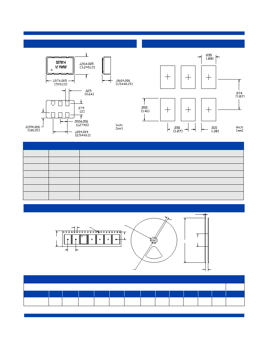
Outline Diagram
Pad Layout
Tape and Reel
A
E
C
D
B
G
F
J
L
I
K
H
Tape Dimensions
Reel Dimensions
# Per Reel
Product A B C D E
F
G
H
I
J
K
L
VC-800
12 5.5 1.5
4
8
1.78
20.6
13 55 6 12.4
178
500
Tape and Reel Dimensions (mm)
1
2
3
4
5
6
Pin #
Symbol
Function
1
VC
Control Voltage
2
Tri-state
Logic low disables output. Logic high or N/C enables output waveform.
3
GND
Ground
4
f
O
Output Frequency
5
CMOS/TTL
Logic low for CMOS optimized symmetry. Logic high or N/C for TTL optimized symmetry.
6
V
DD
Supply Voltage
Pin Out

4
VC-800 Voltage Controlled Crystal Oscillator
Vectron International ∑
267 Lowell Road, Hudson, NH 03051
∑ Tel: 1-88-VECTRON-1 ∑ Fax: 1-888-FAX-VECTRON
Absolute Maximum Ratings
Power Supply
V
DD
6
Vdc
Storage Temperature
Tstorage
-55/125
∞C
Voltage Control Range
V
C
0 to V
DD
V
Stresses in excess of the absolute maximum ratings can permanently damage the device. Functional operation is
not implied at these or any other conditions in excess of conditions represented in the operational sections of this
data sheet. Exposure to absolute maximum ratings for extended periods may adversely affect device reliability.
-200.0
-150.0
-100.0
-50.0
0.0
50.0
100.0
150.0
200.0
0.30
0.60
0.90
1.20
1.50
1.80
2.10
2.40
2.70
3.00
Control Voltage (volts)
Frequency Pull (ppm)
Parameter
Symbol
Ratings
Unit
Figure 3. Typical Frequency Pull Versus Control Voltage, 35.328MHz Output, 3.3 Volt Supply
VC-800 Voltage Controlled Crystal Oscillator
5
Reliability
Environmental Compliance
ESD Ratings
The VC-800 is capable of meeting the following qualification tests.
Mechanical Shock
MIL-STD-883 Method 2002
Mechanical Vibration
MIL-STD-883 Method 2007
Solderability
MIL-STD-883 Method 2003
Gross and Fine Leak
MIL-STD-883 Method 1014
Resistance to Solvents
MIL-STD-883 Method 2016
Handling Precautions
Although ESD protection circuitry has been designed into the the VC-800, proper precautions should be
taken when handling and mounting. VI employs a Human Body Model and a Charged-Device Model
(CDM) for ESD susceptibility testing and design protection evaluation. ESD thresholds are dependent on
the circuit parameters used to define the model. Although no industry wide standard has been adopted
for the CDM, a standard HBM of resistance=1.5kohms and capacitance = 100pF is widely used and
therefore can be used for comparison purposes.
Human Body Model
1500
MIL-STD-883 Method 3115
Charged Device Model
1000
JESD 22-C101
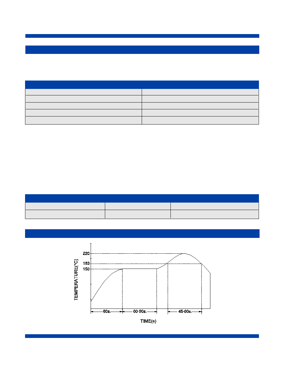
Recommended Solder Reflow Profile
Vectron International ∑
267 Lowell Road, Hudson, NH 03051
∑ Tel: 1-88-VECTRON-1 ∑ Fax: 1-888-FAX-VECTRON
Model
Minimum
Conditions
Parameter
Conditions