 | –≠–ª–µ–∫—Ç—Ä–æ–Ω–Ω—ã–π –∫–æ–º–ø–æ–Ω–µ–Ω—Ç: VDLHLA | –°–∫–∞—á–∞—Ç—å:  PDF PDF  ZIP ZIP |

Product Data Sheet
V-Type
Voltage Controlled Crystal Oscillator (VCXO)
Features
∑ Output Frequencies to 77.760 MHz
∑ 5.0 or 3.3 volt operation
∑ Tri-State Output
∑ Jitter Performance <6 ps rms (freq >12MHz)
∑ VCXO with SwitchableTTL/CMOS Output
∑ Robust 6 contact Leadless Ceramic Chip Carrier
∑ 7.49 x 5.08 x 1.8 mm Surface Mount Device
∑ Absolute Pull Range Performance to 100 ppm
∑ Commercial and Industrial Temperature Range
∑ EIA Compatible Tape and Reel Packaging
Applications
∑ xDSL Customer Premise Equipment (CPE)
∑ Cable Modems
∑ HFC Subscriber Equipmemt
∑ ATM/SONET/SDH applications
Description
The VI V-Type Voltage Controlled Crystal
Oscillator (VCXO) is a quartz-stabilized
square-wave generator with selectable TTL or
CMOS output. The device is hermetically
sealed in a leadless ceramic chip carrier with
6 contact pads.
The V-Type's ultra small footprint and low pro-
file make it ideally suited to applications where
space is limited or where backside assembly
is required.

V-Type Voltage Controlled Crystal Oscillator (VCXO)
Vectron International ∑ 166 Glover Avenue, Norwalk, CT 06856 ∑ Tel: 1-88-VECTRON-1 ∑ Fax: 1-888-FAX-VECTRON
Pin Information
Table 1.
1
Vc Control
Voltage.
2
2
TTL/CMOS
1
TTL logic low for CMOS optimized symmetry
TTL logic high or no connection for TTL optimized symmetry.
3
GND
Case/circuit ground.
4
Output
Output waveform.
5
2
Tri-state
TTL logic low diables output.
TTL logic high or no connection enables output waveform.
6
V
DD
Supply Voltage, 5 V ±10%, or 3.3V ±10%
Pin # Symbol Name/Function
1. This silicon oscillator is fabricated in CMOS technology and
its output waveform will swing between ground and VDD for
all but the highest frequency applications. To account for the
difference in switching thresholds between TTL logic (1.40 V)
and CMOS logic (VDD/2), the TTL/CMOS lead modifies the
"on time" of the oscillator for maximum symmetry about the
TTL or CMOS logic threshold. TTL logic low provides wave-
form symmetry for CMOS. TTL logic high or no connection pro-
vides waveform symmetry for TTL. At output frequencies less
than 12 MHz, this option is not provided as the waveform tran-
sition times are small compared to the period. Hence, for fo
<12 MHz this pin should be grounded for electrical isolation.
2. Alternate Pin Configuration for Tri-state Control on Pin 2
and TTL/CMOS on pin 5. Alternate Configuration is indicated
by last letter of part code "D" for TriState Pin 2 and TTL/CMOS
on pin 5.
Table 2. Performance Specifications
1 A 0.1 uF low frequency tantalum bypass capacitor in parallel with a
0.01 uF high-frequency ceramic capacitor is recommended.
2 Figure 1 defines these parameters. Figure 2 illustrates the equiva-
lent five-gate MTTL load and operating conditions under which
these parameters are specified.
3 Symmetry is defined as (ON TIME/PERIOD), with VS = 1.4 V for
TTL or VS = 2.5 V for CMOS. per Figure 1.
Supply Voltage' (5V or 3.3V)
V
DD
0.9*V
DD
1.1*V
DD
V
Supply Current (Frequency Dependent)
I
DD
See Figures 7,8
mA
OutputVoltage Levels (V
DD
= 4.5V):
Output Logic High
2
V
OH
0.8*V
DD
-
V
Output Logic Low
2
V
OL
-
0.1*V
DD
V
Transition Times
2
:
Rise Time
t
R
5
ns
Fall Time
t
F
5
ns
Symmetry or Duty Cycle
3
SYM
See figure 3, 4
%
Nominal Output Frequency (see ordering info)
fo
1.024
77.760
MHz
Control Voltage (5v), test conditions for APR
Vc
0.5
4.5
V
Control Voltage (3.3v), test conditions for APR
Vc
0.3
3.0
V
Control Voltage
Vc
0
V
DD
V
Absolute Pull Range (see ordering info)
APR
±20 to ±100
Leakage Current of Control Input
Ivcxo
-1.0
1.0
uA
Control Voltage Bandwidth (-3 dB,V
C
=2.50V)
BW
10
-
kHz
Parameter
Symbol
Min
Max
Unit
2

V-Type Voltage Controlled Crystal Oscillator (VCXO)
Vectron International ∑ 166 Glover Avenue, Norwalk, CT 06856 ∑ Tel: 1-88-VECTRON-1 ∑ Fax: 1-888-FAX-VECTRON
Electrical Specifications
Figure 1. Output Waveform
*Includes probe
and test jig
capacitance
Figure 2. Output Test Conditions
(T
amb
= 25 ±5∞C)
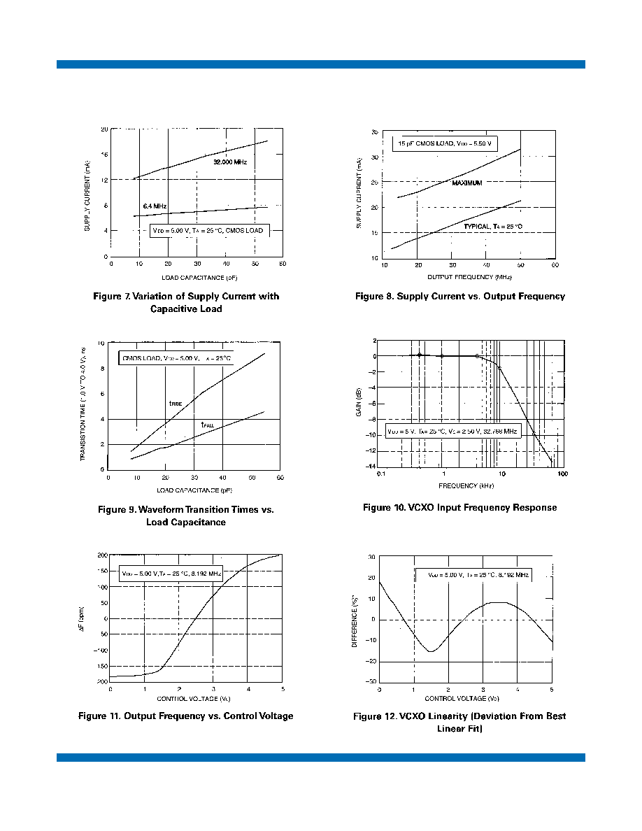
Characteristic Curves
3
Table 3: Typical Single-Side Band Phase Noise Data (dBc/Hz)
Offset From Carrier
VCXO Center Frequency
6.176MHz
12.288MHz
19.440MHz
32.768MHz
39.3216MHz
44.736MHz
51.840MHz
10 Hz
-80
-70
-70
-68
-63
-63
-63
100 Hz
-109
-100
-100
-98
-93
-93
-93
1 KHz
-134
-129
-129
-125
-122
-122
-122
10 KHz
-147
-145
-145
-147
-144
-144
-144
100 KHz
-152
-152
-152
-152
-151
-151
-151
V-Type Voltage Controlled Crystal Oscillator (VCXO)
Vectron International ∑ 166 Glover Avenue, Norwalk, CT 06856 ∑ Tel: 1-88-VECTRON-1 ∑ Fax: 1-888-FAX-VECTRON
Characteristic Curves
(continued)
4

V-Type Voltage Controlled Crystal Oscillator (VCXO)
Vectron International ∑ 166 Glover Avenue, Norwalk, CT 06856 ∑ Tel: 1-88-VECTRON-1 ∑ Fax: 1-888-FAX-VECTRON
Table 4. Absolute Pull Range (APR)
Absolute Frequency Pull Range:
APR
-
-
ppm from f
o
Control Voltage, Vc = 0.50V for 5V
-
-APR
-
ppm from f
o
Control Voltage, Vc = 4.50V for 5V
-
+APR
-
ppm from f
o
Control Voltage, Vc = 0.30V for 3.3V
-
-APR
-
ppm from f
o
Control Voltage, Vc = 3.00V for 3.3V
-
+APR
-
ppm from f
o
Parameter
Symbol
Min
Max
Unit
Absolute pull range (APR) is specified by the fourth character of the
product code (seeTable 5). The APR is the minimum guaranteed fre-
quency shift from fo over variations in temperature, aging, power sup-
ply, and load. Both frequency and environment limit the specified APR.
With Vc between 0.5 V and 4.5 V, total pull range for the V-Type
VCXO is typically between 200 ppm and 400 ppm. A 50 ppm APR
V-Type VCXO will fully track a 50 ppm source oscillator or other 50
ppm reference under all specified environmental conditions.
Mechanical Shock
MIL-STD-883C, 2002.3 B
Mechanical Vibration
MIL-STD-883C, 2007.1 A
Lead Solderability
MIL-STD-883C, 2003.5
Gross Leak
MIL-STD-883C, 1014.7
Fine Leak
MIL-STD-883C, 1014.7
StorageTemperature
-55 ∞C to 125 ∞C
5
Parameter
Conditions
Table 5. Mechanical and Environmental Compliance
Oscillator Aging
Quartz stabilized oscillators typically exhibit a change in out-
put frequency with age. The major factors that contribute to
this change are variations in the mechanical stress applied
to the quartz crystal and mass-loading of foreign material
upon the quartz crystal.
As the oscillator ages, relaxation of the crystal's mounting
stress can lead to frequency variation. In some oscillator
products, additional variations may be brought about by the
transfer of external environmental stress through the device
package and crystal mounting arrangement. VI has mini-
mized these two effects through the use of a state-of-the-art
miniature AT-Cut rectangular resonator. This crystal allows a
mounting arrangement that results in minimal relaxation and
very little environmental stress transfer.
Mass-loading of the quartz resonator, which generally drives
the frequency lower, is a result of outgassing of materials
within a hermetic package or contamination from external
materials in a less than hermetic device. In general, higher fre-
quency resonators are more susceptible to this aging mecha-
nism. VI has minimized the V-Type's sensitivity to these effects
by ensuring the hermetic integrity of the package design and
by minimizing the parts count in the device. By using monolith-
ic IC technology, the component count is reduced and the
amount of material likely to outgas is minimized.
Under normal operating conditions with an operating tem-
perature of 40∞C, the V-Type VCXO will typically exhibit
2ppm aging in its first year of operation.The device is then
expected to exhibit 1ppm aging the following year and will
continue a logarithmic decline for each year there after.