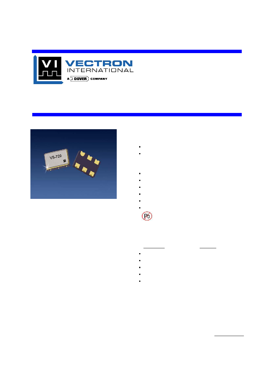
VS-720 Voltage Controlled SAW Oscillator
Vectron International, 267 Lowell Rd, Hudson NH 03051-4916
Tel: 1-88-VECTRON-1
Website: www.vectron.com
PRELIMINARY DATASHEET
VS-720
Voltage Controlled SAW Oscillator
Features
Industry Standard Package, 5.0 x 7.5 x 2.0 mm
ASIC Technology For Ultra Low Jitter
0.100 ps-rms typical across 12 kHz to 20 MHz BW
0.120 ps-rms typical across 50 kHz to 80 MHz BW
Output Frequencies from 150 MHz to 800 MHz
3.3 V Operation
LV-PECL or LVDS Configuration with Fast Transition Times
Complementary Outputs
Output Disable Feature
Improved Temperature Stability over Standard VCSO
Product is free of lead and compliant to
EC RoHS Directive
Applications
PLL circuits for Clock Smoothing and Frequency Translation
Description
Standard
1-2-4 Gigabit Fibre Channel
INCITS 352-2002
10 Gigabit Fibre Channel
INCITS 364-2003
10GbE LAN / WAN
IEEE 802.3ae
OC-192
ITU-T G.709
SONET / SDH
GR-253-CORE Issue3
Description
The VS-720 is a Voltage Controlled SAW Oscillator that
achieves low phase noise and very low jitter performance.
The VS-720 is housed in an industry standard 6-Pad leadless
ceramic package that is hermetically sealed. Packaging
options include bulk or tape and reel
Page 1 of 7
Rev: 09 Jan 2006
VS-720 Voltage Controlled SAW Oscillator
Electrical Performance
Parameter
Symbol
Minimum
Typical
Maximum
Units
Notes
Frequency
Nominal Frequency
Absolute Pull Range
Linearity
Gain Transfer (See Pg 5)
Temperature Stability
f
N
APR
Lin
K
V
f
STAB
150
50
+75
20
800
�10
MHz
ppm
%
ppm/V
ppm
1,2,3
1,2,8
2,4,8
2,8
1
Supply
Voltage
Current (No Load)
V
CC
I
CC
2.97
3.3
55
3.63
70
V
mA
2,3
3
Outputs
Mid Level - LVPECL
Swing LVPECL
Mid Level - LVDS
Swing LVDS
Current
Rise Time
Fall Time
Symmetry
Jitter (12 kHz 20 MHz BW) 622.08 MHz
Jitter (50 kHz 80 MHz BW) 622.08 MHz
I
OUT
t
R
t
F
SYM
J
J
Vcc-1.4
450
V
CC
-2.4
250
45
Vcc-1.25
600
Vcc-2.3
350
50
0.100
0.120
Vcc-1.0
750
V
CC
-2.5
450
20
500
500
55
0.250
0.300
V
mV-pp
V
mV-pp
mA
ps
ps
%
ps-rms
ps-rms
2,3
2,3
2,3
2,3
6
5,6
5,6
2,3
6,7
6,7
Period Jitter, RMS (622.08 MHz)
J
3.0
4.0
ps-rms
9
Period Jitter, Peak - Peak (622.08 MHz)
J
20
30
ps pk-pk
9
Control Voltage
Control Voltage Range for APR
Control Voltage Input Impedance
Control Voltage Modulation BW
V
C
Z
IN
BW
0.3
75
50
3.0
V
K
KHz
2,8
6
6
Operating Temp. (Ordering Option)
T
OP
0/70,-20/70 or -40/85
�C
1,3
Package Size
5.0 x 7.5 x 2.0
mm
1. See Standard Frequencies and Ordering Information tables (Pg 7) for more specific information
2. Parameters are tested with production test circuit below (Fig 1).
3. Parameters are tested at ambient temperature with test limits guard-banded for specified operating temperature.
4. Measured as the maximum deviation from the best straight-line fit, per MIL-0-55310.
5. Measured from 20% to 80% of a full output swing (Fig 2).
6. Not tested in production, guaranteed by design, verified at qualification.
7. Integrated across stated bandwidth per GR-253-CORE Issue3.
8. Tested with Vc = 0.3V to 3.0V unless otherwise stated in part description
9. Broadband Period Jitter measured using Lecroy Wavemaster 8600A 6 GHz Oscilloscope, 250K samples taken
Vectron International 166 Glover Avenue, Norwalk CT 06856-5160 Tel: 1-88-VECTRON-1
Website: www.vectron.com
Figure 1. Test Circuit
Figure 2. 10K LV-PECL Waveform
Vcc - 1.6V
Vcc - 1.3V
Vcc - 1.0V
80%
20%
SYM = 100 x t
A
/ t
B
t
R
t
F
t
A
t
B
Page 3 of 7
Rev: 09 Jan 2006
1
2
3
6
5
4
50
50
Test Circuit Notes:
1) To Permit 50 Measurement of Outputs, all DC Inputs are Biased Down 1.3V.
2) All Voltage Sources Contain Bypass Capacitors to Minimize Supply Noise.
3) 50
Terminations are Within Test Equipment.
(-1.3V to +2.0V)
(-1.3V, +2.0V)
(-1.3V)
(+2.0V)
COutput
Output
Enable, Disable
VS-720 Voltage Controlled SAW Oscillator
Vectron International 166 Glover Avenue, Norwalk CT 06856-5160 Tel: 1-88-VECTRON-1
Website: www.vectron.com
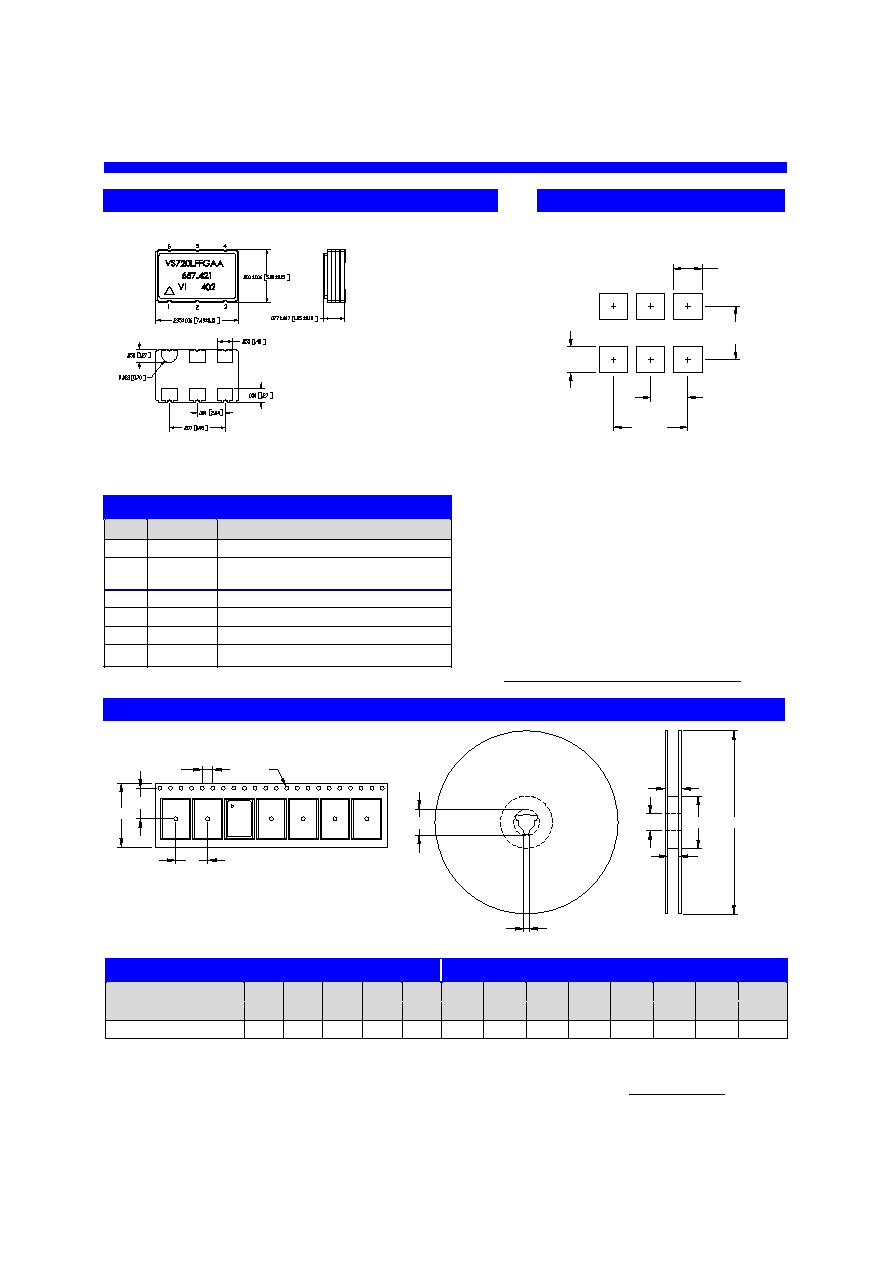
Outline Diagram
Suggested Pad Layout
mm
[inch]
5.08
[0.200]
2.54
[0.100]
1.78
[0.070]
3.66
[0.144]
1.96
[0.077]
Standard Pin Out
Pin
Symbol
Function
1
V
C
VCXO
2
OE
1
Enable = LV-CMOS logic 0 or Ground,
Disable = LV-CMOS logic 1
3
GND
Case and Electrical Ground
4
Output
Output
5
COutput
Complementary Output
6
V
CC
Power Supply Voltage (3.3V �10%)
Note 1: For proper operation disable pin can not be left floating
. See page 7 for alternative input logic option
Tape and Reel (EIA-481-2-A)
Tape Dimensions (mm)
Reel Dimensions (mm)
Dimension
W
F
Do
Po
P1
A
B
C
D
N
W1
W2
# Per
Tolerance
Typ
Typ
Typ
Typ
Typ
Typ
Min
Typ
Min
Min
Typ
Max
Reel
VS-720
16
7.5
1.5
4
8
178
1.5
13
20.2
50
16.4
22.4
200
Po
W
A
N
F
P1
W1
W2
C
B
D
�Do
Page 3 of 7
Rev: 09 Jan 2006

VS-720 Voltage Controlled SAW Oscillator
Absolute Maximum Ratings
Parameter
Symbol
Ratings
Unit
Power Supply
V
CC
0 to 4
V
Output Current
Iout
25
mA
Voltage Control Range
V
C
0 to V
CC
V
Storage Temperature
TS
-55 to 125
C
Soldering Temp/Time
T
LS
260/40
C/sec
Stresses in excess of the absolute maximum ratings can permanently damage the device. Functional operation
is not implied at these or any other conditions in excess of conditions represented in the operational sections of
this datasheet. Exposure to absolute maximum ratings for extended periods may adversely affect device
reliability. Permanent damage is also possible if OD or Vc is applied before Vcc.
Suggested Output Load Configurations
4
3
240
0.01 F
1
6
2
Gnd
OD
5
Vc
0.10 F
+3.3V
240
100
Z = 50
Z = 50
COutput
Vcc
Output
Gnd
Vc
OD
Output
240
3
4
240
COutput
2
1
5
6
Vcc
0.01 F
0.10 F
+3.3V
OD
-1.3V
COutput
Output
4
3
2
5
Vc
0.01 F
1
6
Vcc
0.10 F
+2.0V
LV-PECL to LV-PECL:
For short transmission lengths, the power
consumption could be reduced by removing the 100 resistor and
doubling the value of the pull down resistors.
Functional Test:
Allows standard power supply configuration.
Since AC coupled, the LV-PECL levels cannot be measured.
LV-PECL to LVDS:
Restricted for short transmission lengths.
Configuration may require modification depending on LVDS receiver.
Gnd
3
Output
4
Z = 50
+3.3V
COutput
OD
Vc
2
1
5
Vcc
6
0.01 F
0.10 F
Z = 50
40
40
150
150
49
49
+3.3V
Production Test:
Allows direct DC coupling into 50 measurement
equipment. Must bias the power supplys as shown. Similar to Figure 1.
0.01 F
0.01 F
Vectron International 166 Glover Avenue, Norwalk CT 06856-5160 Tel: 1-88-VECTRON-1
Website: www.vectron.com
Page 4 of 7
Rev: 09 Jan 2006
VS-720 Voltage Controlled SAW Oscillator
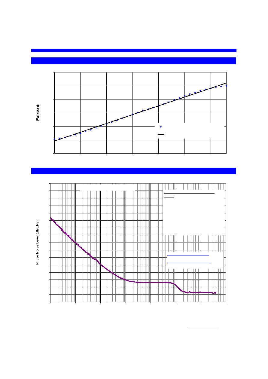
Typical Gain Transfer
-150
-100
-50
0
50
100
150
0.00
0.50
1.00
1.50
2.00
2.50
3.00
Control Voltage (volts)
VS-720 pull, 622 MHz
Linear (VS-720 pull, 622 MHz)
Typical Phase Noise
VS-720-LFF-GAB- 622.0800 MHz
-160
-150
-140
-130
-120
-110
-100
-90
-80
-70
-60
-50
-40
-30
-20
-10
0
10
100
1000
10000
100000
1000000
10000000
100000000
Frequency Offset (Hz)
Phase Noise at Specific Frequency
Offsets
10Hz -46 dBc/Hz
100Hz -80 dBc/Hz
1000Hz -110 dBc/Hz
10kHz -130 dBc/Hz
100kHz -134 dBc/Hz
1MHz -138 dBc/Hz
10MHz -147 dBc/Hz
20MHz -147 dBc/Hz
40MHz -148 dBc/Hz
Jitter OC48 (12kHz to 20MHz)
0.08 ps-rms or 0.56 ps-pp
Jitter OC192 (50kHz to 80MHz)
0.11 ps-rms or 0.80 pp-rms
Page 5 of 7
Vectron International 166 Glover Avenue, Norwalk CT 06856-5160 Tel: 1-88-VECTRON-1
Website: www.vectron.com
Rev: 09 Jan 2006