VIA Technologies, Inc
.
VT8225
1045 Mission Court. 8th. Fl., No. 533
Fremont, CA 94539 Chung-cheng Rd.,Hsin-tien
USA Taipei, Taiwan, R.O.C.
TEL: 1-510-683-3300 FAX: 1-510-683-3301 TEL: 886-2-218-5452 FAX: 886-2-218-5453
-1-
VT8225 Clock Generator
Date: July 5, 1994
Features
Generates essential clock signals for the motherboard
4V to 7V operating supply range
Supports 80286, 80386 and 80486 based designs
Wide range of selectable output frequencies
< 2ns skew between CPU and 2X CPU clock outputs
Single low cost crystal (14.318Mhz) used as reference frequency
Smooth transition on frequency switching
50% duty cycle
Power down mode for low power consumption
TTL or CMOS compatible outputs with 12mA drive capability
Low, short and long term jitter
14 pin DIP and 14 pin SOIC (300 mil body) package options
Description
The VT8225 is a universal clock generator for motherboard design. The product at a glimpse:
1. Generates all kinds of required clocks for CPU and bus operation from 6 Mhz to 80 Mhz.
2. Eliminates at least two oscillators, which are oscillators for CPU and 14.318MHz oscillator.
3. Simplifies inventory: VT8225 covers required main clock for the motherboard design.
4. Provides a reliable clock for the PLL design.
5. Is pin-to-pin compatible to oscillator.
VIA Technologies, Inc.
VT8225
-2-
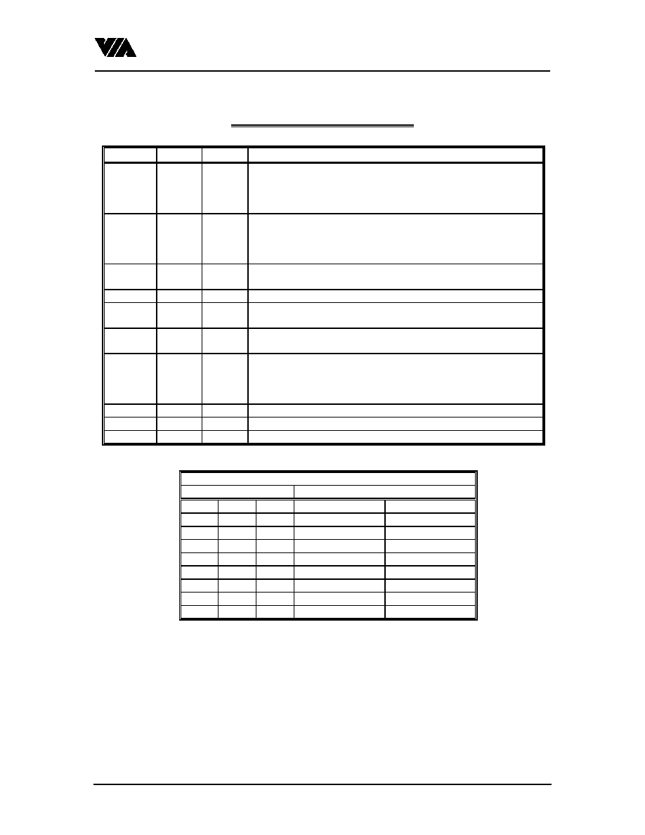
VT8225 Signal Description
Symbol Pin No.
Type
Functions
X1
X2
2
3
I
I/O
These pins form an on-chip reference oscillator when connected to
terminals of an external parallel resonant crystal (norminally
14.318Mhz). X1 may also serve as input for an externally
generated reference signal.
S0
S1
S2
S3
4
5
10
9
I
I
I
I
Frequency select inputs. These inputs control the MCLK frequency
selection. All these inputs have internal pull-ups. Table 1 below
shows the output frequency selection conditions.
MCLK
8
O
Master clock output. Programmable output frequencies can
be selected using So-S3.
RESET#
11
O
Chip reset, negative true.
TS
1
I
Tri-state input pin. When high, all outputs are tri-stated. When low
outputs are enabled. This pin has an internal pull-down.
OSC
13
O
14.31818 Mhz output. Buffered output of on-chip reference
oscillaor or externally provided reference.
PD
6
O
This is the phase detector output for the clock generator. It is
single-ended, tri-state output for use as loop error signal. A 0.1uF
capacitor to ground should be connected from this pin to form the
loop filter.
VSS
7
Ground
Digital Negative power supply.
AVSS
12
Ground
Analog Negative power supply.
VDD
14
Power
Positive power supply.
MCLK FREQUENCY SELECTION
INPUTS
MCLK OUTPUT
S2
S1
S0
S3=1 (Bank 1)
S3=0 (Bank 0)
0
0
0
8 Mhz
16 Mhz
0
0
1
20 Mhz
40 Mhz
0
1
0
25 Mhz
50 Mhz
0
1
1
40 Mhz
80 Mhz
1
0
0
33.3 Mhz
66.6 Mhz
1
0
1
50 Mhz
100 Mhz
1
1
0
4 Mhz
8 Mhz
1
1
1
2 Mhz
4 Mhz
Table 1 clock frequency selection
Note : The smooth transition of frequency change is only allowed within the same selection bank.
VIA Technologies, Inc.
VT8225
-3-
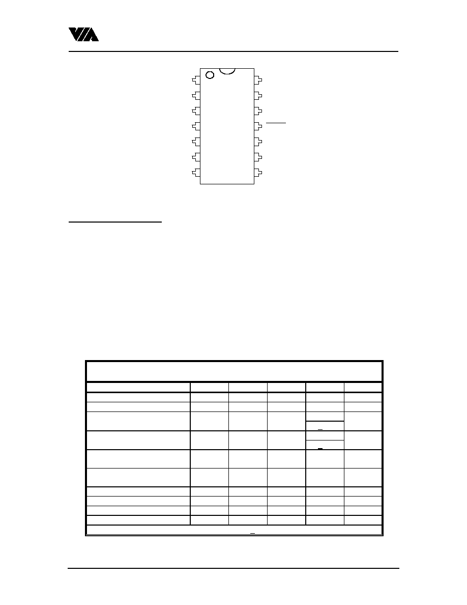
TS
S0
S1
PD
VSS
VDD
S2
S3
MCLK2
1
2
3
4
5
6
7
14
13
12
11
10
9
8
X1
X2
OSC
AVSS
RESET
Figure 1: Connection Diagram for Plastic Dip or SOIC Package
MAXIMUM RATINGS
Voltage relative to VSS :.................-0.3V TO 7V
Voltage relative to VDD:.................0.3V
Storage temperature:........................-65oC to 150oC
Ambient temperature: ......................-55oC to +125oC
Recommended Operating Range: ....4V - 7V
This device contains circuitry to protect the inputs against damage due to high static voltages or
electric field; however, precautions should be taken to avoid application of any voltage higher than the
maximum rated voltages to this circuit. For proper operation, Vin and Vout should be constrained to the
range:
V
SS
< (Vin or Vout) < V
DD
Unused inputs must always be tied to an appropriate logic voltage level (either V
SS
or V
DD
).
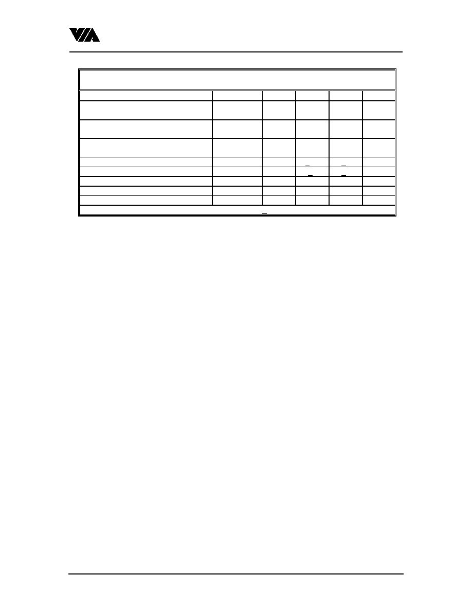
ELECTRICAL CHARACTERISTICS
Characteristic
Symbol
Min
Typ
Max
Units
Input Low Voltage
V
IL
-
-
0.8
Vdc
Input High Voltage
V
IH
2.0
-
-
Vdc
Input Low Current
I
IL
-
-
5
�
A
With Pull-up or Pull-down
+ 50
Input High Current
I
IH
-
-
5
�
A
With Pull-up or Pull-down
+ 50
Output Low Voltage
I
OL
= 12mA
V
OL
-
-
0.4
Vdc
Output High Voltage
I
OH
= 12mA
V
OH
2.4
-
-
Vdc
Tri-State Leakage Current
I
OZ
-
-
10
�
A
Static Supply Current
I
DD
-
-
10
�
A
Dynamic Supply Current
I
CC
-
-
35
mA
Short Circuit Current
I
SC
25
-
mA
VDD = 5V + 10%, TA = -40
o
C to +85
o
C, CL = 50pF
VIA Technologies, Inc.
VT8225
-4-
SWITCHING CHARACTERISTICS
Characteristics
Symbol
Min
Typ
Max
Units
Output Rise(0.8v-2.0v) and Fall Time
(2.0v-0.8v)
t
TLH
, t
THL
-
2
ns
Output Enable
TS to All Output
t
Z
35
ns
Duty Cycle
All Output
d
T
40
48/52
60
%
Jitte, One Sigma
t
J1S
+0.5
+2
%
Jitter, Absolute
t
ABS
+3
+5
%
Frequency Transition Time
t
FT
20
ms
Power Up Time
t
PU
15
40
ms
Input Rise and Fall Times OSCIN
t
TLH
,t
THL
-
3
1
us
VDD = 5V + 10%, TA = -40
o
C to +85
o
C, CL = 50pF