 | –≠–ª–µ–∫—Ç—Ä–æ–Ω–Ω—ã–π –∫–æ–º–ø–æ–Ω–µ–Ω—Ç: 4N33-X007 | –°–∫–∞—á–∞—Ç—å:  PDF PDF  ZIP ZIP |

4N32/ 4N33
Document Number 83736
Rev. 1.4, 26-Jan-05
Vishay Semiconductors
www.vishay.com
1
i179005
1
2
3
6
5
4
B
C
E
A
C
NC
Pb
Pb-free
e3
Optocoupler, Photodarlington Output, High Gain, With Base
Connection
Features
∑ Very high current transfer ratio, 500 % Min.
∑ High isolation resistance, 10
11
Typical
∑ Standard plastic DIP package
∑ Lead-free component
∑ Component in accordance to RoHS 2002/95/EC
and WEEE 2002/96/EC
Agency Approvals
∑ UL1577, File No. E52744 System Code H or J,
Double Protection
∑ DIN EN 60747-5-2 (VDE0884)
DIN EN 60747-5-5 pending
Available with Option 1
∑ BSI IEC60950 IEC60065
Description
The 4N32 and 4N33 are optically coupled isolators
with a gallium arsenide infrared LED and a solicon
photodarlington sensor.
Switching can be achieved while maintaining a high
degree of isolation between driving and load circuits.
These optocouplers can be used to replace reed and
mercury relays with advantages of long life, high
speed switching and elimination of magnetic fields.
Order Information
For additional information on the available options refer to
Option Information.
Absolute Maximum Ratings
T
amb
= 25 ∞C, unless otherwise specified
Stresses in excess of the absolute Maximum Ratings can cause permanent damage to the device. Functional operation of the device is
not implied at these or any other conditions in excess of those given in the operational sections of this document. Exposure to absolute
Maximum Rating for extended periods of the time can adversely affect reliability.
Input
Part
Remarks
4N32
CTR > 500 %, DIP-6
4N33
CTR > 500 %, DIP-6
4N32-X007
CTR > 500 %, SMD-6 (option 7)
4N32-X009
CTR > 500 %, SMD-6 (option 9)
4N33-X007
CTR > 500 %, SMD-6 (option 7)
4N33-X009
CTR > 500 %, SMD-6 (option 9)
Parameter
Test condition
Symbol
Value
Unit
Peak reverse voltage
V
R
3.0
V
Forward continuous current
I
F
60
mA
Power dissipation
P
diss
100
mW
Derate linearly
from 55 ∞C
1.33
mW/∞C

www.vishay.com
2
Document Number 83736
Rev. 1.4, 26-Jan-05
4N32/ 4N33
Vishay Semiconductors
Output
Coupler
Electrical Characteristics
T
amb
= 25 ∞C, unless otherwise specified
Minimum and maximum values are testing requirements. Typical values are characteristics of the device and are the result of engineering
evaluation. Typical values are for information only and are not part of the testing requirements.
Input
Parameter
Test condition
Symbol
Value
Unit
Collector-emitter breakdown voltage
BV
CEO
30
V
Emitter-base breakdown voltage
BV
EBO
8.0
V
Collector-base breakdown voltage
BV
CBO
50
V
Emitter-collector breakdown voltage
BV
ECO
5.0
V
Collector (load) current
I
C
125
mA
Power dissipation
P
diss
150
mW
Derate linearly
2.0
mW/∞C
Parameter
Test condition
Symbol
Value
Unit
Total dissipation
P
tot
250
mW
Derate linearly
3.3
mW/∞
Isolation test voltage (between
emitter and detector, Standard
Climate: 23 ∞C/ 50 %RH, \\nDIN
500 14)
V
ISO
5300
V
RMS
Leakage Path
7.0
mm min.
Air Path
7.0
mm min.
Isolation Resistance
V
IO
= 500 V, T
amb
= 25 ∞C
R
IO
10
12
V
IO
= 500 V, T
amb
= 100 ∞C
R
IO
10
11
Storange temperature
T
amb
- 55 to + 150
∞C
Operating temperature
T
stg
- 55 to + 100
∞C
Lead soldering time
at 260 ∞C
10
s
Parameter
Test condition
Symbol
Min
Typ.
Max
Unit
Forward voltage
I
F
= 50 mA
V
F
1.25
1.5
V
Reverse current
V
R
= 3.0 V
I
R
0.1
100
µ
Capacitance
V
R
= 0 V
C
O
25
pF

4N32/ 4N33
Document Number 83736
Rev. 1.4, 26-Jan-05
Vishay Semiconductors
www.vishay.com
3
Output
1)
Indicates JEDEC registered values
Coupler
Current Transfer Ratio
Switching Characteristics
Typical Characteristics (Tamb = 25
∞C unless otherwise specified)
Parameter
Test condition
Symbol
Min
Typ.
Max
Unit
Collector-emitter breakdown
voltage
1)
I
C
= 100
µA, I
F
= 0
BV
CEO
30
V
Collector-base breakdown
voltage
1)
I
C
= 100
µA, I
F
= 0
BV
CBO
50
V
Emitter-base breakdown
voltage
1)
I
C
= 100
µA, I
F
= 0
BV
EBO
8.0
V
Emitter-collector breakdown
voltage
1)
I
C
= 100
µA, I
F
= 0
BV
ECO
5.0
10
V
Collector-emitter leakage
current
V
CE
= 10 V, I
F
= 0
I
CEO
1.0
100
nA
I
C
= 0.5 mA, V
CE
= 5.0 V
h
FE
13
Parameter
Test condition
Symbol
Min
Typ.
Max
Unit
Colector emitter saturation
voltage
V
CEsat
1.0
V
Coupling capacitance
1.5
pF
Parameter
Test condition
Symbol
Min
Typ.
Max
Unit
Current Transfer Ratio
V
CE
= 10 V, I
F
= 10 mA,
CTR
500
%
Parameter
Test condition
Symbol
Min
Typ.
Max
Unit
Turn on time
V
CC
= 10 V, I
C =
50 mA
t
on
5.0
µs
Turn off time
I
F
= 200 mA, R
L
= 180
t
off
100
µs
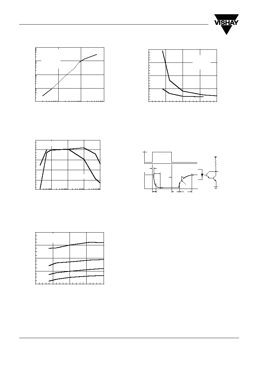
Figure 1. Normalized Non-saturated and Saturated CTR
CE
vs.
LED Current
i4n32-33_02
.1
1
10
100
1000
0.0
0.2
0.4
0.6
0.8
1.0
1.2
Vce =1V
Vce = 5 V
IF - LED Current - mA
NCTRce
-
N
ormalized
CTRce
Vce = 5 V
IF = 10 mA
Ta = 25∞C
Normalized to:
Figure 2. Normalized Non-Saturated and Saturated Collector-
Emitter Current vs. LED Current
i4n32-33_03
100
1
.1
.001
.01
.1
1
10
Vce = 1V
Vce = 5 V
IF - LED Current - mA
NIce
-
Normalized
Ice
Ta = 25∞C
IF = 10 mA
Vce = 5 V
Normalized to:
10
www.vishay.com
4
Document Number 83736
Rev. 1.4, 26-Jan-05
4N32/ 4N33
Vishay Semiconductors
Figure 3. Normalized Collector-Base Photocurrent vs. LED
Current
Figure 4. Non-Saturated and Saturated HFE vs. Base Current
Figure 5. Low to High Propagation Delay vs. Collector Load
Resistance and LED Current
i4n32-33_04
.1
1
1 0
100
.001
.01
.1
1
10
IF - LED Current - mA
NIcb
-
N
ormalized
Icb
Ta = 25∞C
Vcb = 3.5 V
IF = 10 mA
Normalized to:
i4n32-33_05
.01
.1
1
10
100
0
2000
4000
6000
8000
10000
Vce = 5 V
Vce = 1 V
Ib - Base Current -
µA
HFE
-
Forward
Transfer
Gain
Ta = 25∞C
i4n32-33_06
0
5
10
15
20
0
20
40
60
80
Ta = 25∞C, Vcc = 5V
Vth = 1.5 V
220
i
470
IF - LED Current - mA
tpLH
-
Low/High
Propagation
Delay
-
µ
S
100
1.0 k
Figure 6. High to low Propagation Delay vs. Collector Load
Resistance and LED Current
Figure 7. Switching Waveform and Switching Schematic
i4n32-33_07
0
5
10
15
20
0
5
10
15
20
100
1k
IF - LED Current - mA
tpHL
-
H
igh/Low
Propagation
delay
-
µ
s
Ta = 25∞C
Vcc = 5 V
Vth = 1.5 V
i4n32-33_08
IF
tR
VO
tD
tS
tF
tPHL
tPLH
VTH=1.5 V
VO
RL
VCC
IF

4N32/ 4N33
Document Number 83736
Rev. 1.4, 26-Jan-05
Vishay Semiconductors
www.vishay.com
5
Package Dimensions in Inches (mm)
For 4N32/33..... see DIL300-6 Package dimension in the Package Section.
For products with an option designator (e.g. 4N32-X007 or 4N33-X009)..... see DIP-6 Package dimensions in the Package Section.
DIL300-6 Package Dimensions
DIP-6 Package Dimensions
14770
i178004
.010 (.25)
typ.
.114 (2.90)
.130 (3.0)
.130 (3.30)
.150 (3.81)
.031 (0.80) min.
.300 (7.62)
typ.
.031 (0.80)
.035 (0.90)
.100 (2.54) typ.
.039
(1.00)
Min.
.018 (0.45)
.022 (0.55)
.048 (0.45)
.022 (0.55)
.248 (6.30)
.256 (6.50)
.335 (8.50)
.343 (8.70)
pin one ID
6
5
4
1
2
3
18∞
3∞≠9∞
.300≠.347
(7.62≠8.81)
4∞
typ.
ISO Method A

www.vishay.com
6
Document Number 83736
Rev. 1.4, 26-Jan-05
4N32/ 4N33
Vishay Semiconductors
.315 (8.0)
MIN.
.300 (7.62)
TYP.
.180 (4.6)
.160 (4.1)
.331 (8.4)
MIN.
.406 (10.3)
MAX.
.028 (0.7)
MIN.
Option 7
18494
min.
.315 (8.00)
.020 (.51)
.040 (1.02)
.300 (7.62)
ref.
.375 (9.53)
.395 (10.03)
.012 (.30) typ.
.0040 (.102)
.0098 (.249)
15∞ max.
Option 9

4N32/ 4N33
Document Number 83736
Rev. 1.4, 26-Jan-05
Vishay Semiconductors
www.vishay.com
7
Ozone Depleting Substances Policy Statement
It is the policy of Vishay Semiconductor GmbH to
1. Meet all present and future national and international statutory requirements.
2. Regularly and continuously improve the performance of our products, processes, distribution and
operatingsystems with respect to their impact on the health and safety of our employees and the public, as
well as their impact on the environment.
It is particular concern to control or eliminate releases of those substances into the atmosphere which are
known as ozone depleting substances (ODSs).
The Montreal Protocol (1987) and its London Amendments (1990) intend to severely restrict the use of ODSs
and forbid their use within the next ten years. Various national and international initiatives are pressing for an
earlier ban on these substances.
Vishay Semiconductor GmbH has been able to use its policy of continuous improvements to eliminate the use
of ODSs listed in the following documents.
1. Annex A, B and list of transitional substances of the Montreal Protocol and the London Amendments
respectively
2. Class I and II ozone depleting substances in the Clean Air Act Amendments of 1990 by the Environmental
Protection Agency (EPA) in the USA
3. Council Decision 88/540/EEC and 91/690/EEC Annex A, B and C (transitional substances) respectively.
Vishay Semiconductor GmbH can certify that our semiconductors are not manufactured with ozone depleting
substances and do not contain such substances.
We reserve the right to make changes to improve technical design
and may do so without further notice.
Parameters can vary in different applications. All operating parameters must be validated for each
customer application by the customer. Should the buyer use Vishay Semiconductors products for any
unintended or unauthorized application, the buyer shall indemnify Vishay Semiconductors against all
claims, costs, damages, and expenses, arising out of, directly or indirectly, any claim of personal
damage, injury or death associated with such unintended or unauthorized use.
Vishay Semiconductor GmbH, P.O.B. 3535, D-74025 Heilbronn, Germany
Telephone: 49 (0)7131 67 2831, Fax number: 49 (0)7131 67 2423