6N1135/ 6N1136
Document Number 83909
Rev. 1.5, 26-Oct-04
Vishay Semiconductors
www.vishay.com
1
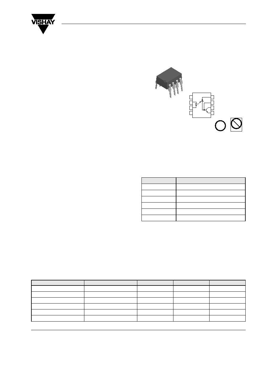
i179081
1
2
3
4
8
7
6
5
C (V
CC
)
NC
A
C
NC
B (V
B
)
C (V
O
)
E (GND)
Pb
Pb-free
e3
High Speed Optocoupler, 1 MBd, Photodiode with Transistor
Output, 110 �C Rated
Features
� Operating Temperature from -55 �C to +110 �C
� Isolation Test Voltage: 5300 V
RMS
� TTL Compatible
� High Bit Rates: 1.0 MBd
� Bandwidth 2.0 MHz
� Open-Collector Output
� External Base Wiring Possible
� Lead-free component
� Component in accordance to RoHS 2002/95/EC
and WEEE 2002/96/EC
Agency Approvals
� UL 1577 - File No. E52744 System Code H or J
� DIN EN 60747-5-2 (VDE0884)
� CUL - File No. E52744, equivalent to CSA bulletin
5A
Description
The 6N1135 and 6N1136 are 110 �C rated optocou-
plers with a GaAIAs infrared emitting diode, optically
coupled with an integrated photo detector which con-
sists of a photo diode and a high-speed transistor in a
DIP-8 plastic package.
Signals can be transmitted between two electrically
separated circuits up to frequencies of 2.0 MHz. The
potential difference between the circuits to be coupled
should not exceed the maximum permissible refer-
ence voltages
Order Information
For additional information on the available options refer to
Option Information.
Absolute Maximum Ratings
T
amb
= 25 �C, unless otherwise specified
Stresses in excess of the absolute Maximum Ratings can cause permanent damage to the device. Functional operation of the device is
not implied at these or any other conditions in excess of those given in the operational sections of this document. Exposure to absolute
Maximum Rating for extended periods of the time can adversely affect reliability.
Input
Part
Remarks
6N1135
CTR
7 %, DIP-8
6N1136
CTR
19 %, DIP-8
6N1135-X007
CTR
7 %, SMD-8 (option 7)
6N1136-X006
CTR
19 %, DIP-8 400 mil (option 6)
6N1136-X007
CTR
19 %, SMD-8 (option 7)
6N1136-X009
CTR
19 %, SMD-8 (option 9)
Parameter
Test condition
Symbol
Value
Unit
Reverse voltages
V
R
5.0
V
Forward current
I
F
25
mA
Peak forward current
t = 1.0 ms, duty cycle 50 %
I
FM
50
mA
Maximum surge forward current t
1.0 �s, 300 pulses/s
I
FSM
1.0
A
Thermal resistance
R
th
700
K/W
Power dissipation
T
amb
= 70 �C
P
diss
45
mW
www.vishay.com
2
Document Number 83909
Rev. 1.5, 26-Oct-04
6N1135/ 6N1136
Vishay Semiconductors
Output
Coupler
Electrical Characteristics
T
amb
= 25 �C, unless otherwise specified
Minimum and maximum values are testing requirements. Typical values are characteristics of the device and are the result of engineering
evaluation. Typical values are for information only and are not part of the testing requirements.
Input
Output
Parameter
Test condition
Symbol
Value
Unit
Supply voltage
V
CC
- 0.5 to 15
V
Output voltage
V
O
- 0.5 to 15
V
Emitter-base voltage
V
EBO
5.0
V
Output current
I
O
8.0
mA
Maximum output current
16
mA
Base current
I
B
5.0
mA
Thermal resistance
300
K/W
Power dissipation
T
amb
= 70 �C
P
diss
100
mW
Parameter
Test condition
Symbol
Value
Unit
Isolation test voltage (between
emitter and detector climate per
DIN 50014 part 2, NOV 74
t = 1.0 s
V
ISO
5300
V
RMS
Storage temperature range
T
stg
- 55 to + 125
�C
Ambient temperature range
T
amb
- 55 to + 110
�C
Soldering temperature
max.
10 s, dip soldering
0.5 mm from case bottom
T
sld
260
�C
Parameter
Test condition
Symbol
Min
Typ.
Max
Unit
Forward voltage
I
F
= 16 mA
V
F
1.6
1.9
V
Breakdown voltage
I
R
= 10
�A
V
BR
5.0
V
Reverse current
V
R
= 5.0 V
I
R
0.5
10
�A
Capacitance
V
R
= 0 V, f = 1.0 MHz
C
I
125
pF
Temperature coefficient, forward voltage
I
F
= 16 mA
V
F
/
T
A
-1.7
mV/�C
Parameter
Test condition
Part
Symbol
Min
Typ.
Max
Unit
Logic low supply current
I
F
= 16 mA, V
O
open, V
CC
= 15 V
I
CCL
150
�A
Supply current, logic high
I
F
= 0 mA, V
O
open, V
CC
= 15 V
I
CCH
0.01
1
�A
Output voltage, output low
I
F
= 16 mA, V
CC
= 4.5 V,
I
O
= 1.1 mA
6N1135
V
OL
0.1
0.4
V
I
F
= 16 mA, V
CC
= 4.5 V,
I
O
= 2.4 mA
6N1136
V
OL
0.1
0.4
V
Output current, output high
I
F
= 0 mA, V
O
= V
CC
= 5.5 V
I
OH
3.0
500
nA
I
F
= 0 mA, V
O
= V
CC
= 15 V
I
OH
0.01
1
�A

6N1135/ 6N1136
Document Number 83909
Rev. 1.5, 26-Oct-04
Vishay Semiconductors
www.vishay.com
3
Coupler
Switching Characteristics
Common Mode Transient Immunity
Parameter
Test condition
Part
Symbol
Min
Typ.
Max
Unit
Capacitance (input-output)
f = 1.0 MHz
C
IO
0.6
pF
Current Transfer Ratio
I
F
= 16 mA, V
O
= 0.4
V, V
CC
= 4.5 V
6N1135
CTR
7
16
%
6N1136
CTR
19
35
%
I
F
= 16 mA, V
O
= 0.5
V, V
CC
= 4.5 V
6N1135
CTR
5
%
6N1136
CTR
15
%
Parameter
Test condition
Part
Symbol
Min
Typ.
Max
Unit
High-low
I
F
= 16 mA, V
CC
= 5.0 V, R
L
= 4.1 k
6N1135
t
PHL
0.3
1.5
�s
I
F
= 16 mA, V
CC
= 5.0 V, R
L
= 1.9 k
6N1136
t
PHL
0.2
0.8
�s
Low-high
I
F
= 16 mA, V
CC
= 5.0 V, R
L
= 4.1 k
6N1135
t
PLH
0.3
1.5
�s
I
F
= 16 mA, V
CC
= 5.0 V, R
L
= 1.9 k
6N1136
t
PLH
0.2
0.8
�s
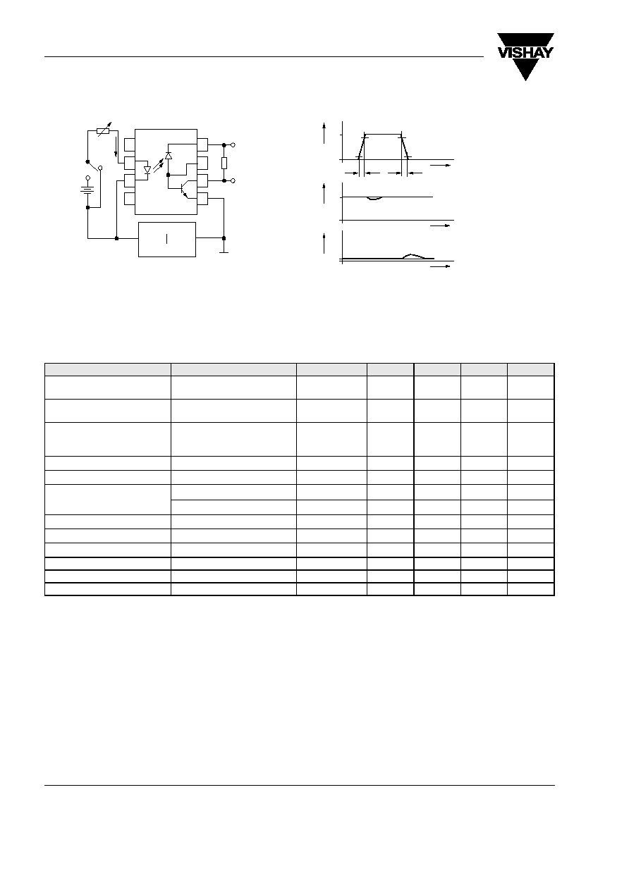
Figure 1. Switching Times
Parameter
Test condition
Part
Symbol
Min
Typ.
Max
Unit
High
I
F
= 0 mA, V
CM
= 10 V
P-P
, V
CC
= 5.0 V, R
L
= 4.1 k
6N1135
| CM
H
|
1000
V/
�s
I
F
= 0 mA, V
CM
= 10 V
P-P
, V
CC
= 5.0 V, R
L
= 1.9 k
6N1136
| CM
H
|
1000
V/
�s
Low
I
F
= 16 mA, V
CM
= 10 V
P-P
, V
CC
= 5.0 V, R
L
= 4.1 k
6N1135
| CM
L
|
1000
V/
�s
I
F
= 16 mA, V
CM
= 10 V
P-P
, V
CC
= 5.0 V, R
L
= 1.9 k
6N1136
| CM
L
|
1000
V/
�s
i6n135_01
V
OL
t
t
5 V
1.5 V
V
O
I
F
t
PLH
t
PHL
1
2
3
4
8
7
6
5
I
F
V
O
R
L
5 V
Pulse generator
Z
O
=50
t
r,
t
f
=5 ns
duty cycle 10%
t
100 �s
C
L
15 pF
I
F
Monitor
100
i
www.vishay.com
4
Document Number 83909
Rev. 1.5, 26-Oct-04
6N1135/ 6N1136
Vishay Semiconductors
Safety and Insulation Ratings
As per IEC60747-5-2, �7.4.3.8.1, this optocoupler is suitable for "safe electrical insulation" only within the safety ratings. Compliance with
the safety ratings shall be ensured by means of protective circuits.
Figure 2. Common-Mode Interference Immunity
Parameter
Test condition
Symbol
Min
Typ.
Max
Unit
Climatic Classification
(according to IEC 68 part 1)
55/110/21
Pollution degree (DIN VDE
0109)
2.0
Comparative tracking index per
DIN IEC112/VDE 0303 part 1,
group IIIa per DIN VDE 6110
175
399
V
IOTM
V
IOTM
8000
V
V
IORM
V
IORM
630
V
Isolation resistance
V
IO
= 500 V, T
amb
= 25 �C
R
IO
10
12
V
IO
= 500 V, T
amb
= 100 �C
R
IO
10
11
P
SI
P
SI
500
mA
I
SI
I
SI
300
mW
T
SI
T
SI
175
�C
Creepage
7.0
mm
Clearance
7.0
mm
Insulation thickness
0.2
mm
i6n135_02
V
CM
V
O
V
O
10 V
5 V
0 V
V
OL
90%
10%
90%
10%
tr
tf
t
t
t
A: I
F
=0 mA
B: I
F
=16 mA
1
2
3
4
8
7
6
5
B
V
FF
I
F
+V
CM
V
O
R
L
5 V
A
Pulse generator
Z
O
=50
t
r,
t
f
=8 ns

6N1135/ 6N1136
Document Number 83909
Rev. 1.5, 26-Oct-04
Vishay Semiconductors
www.vishay.com
5
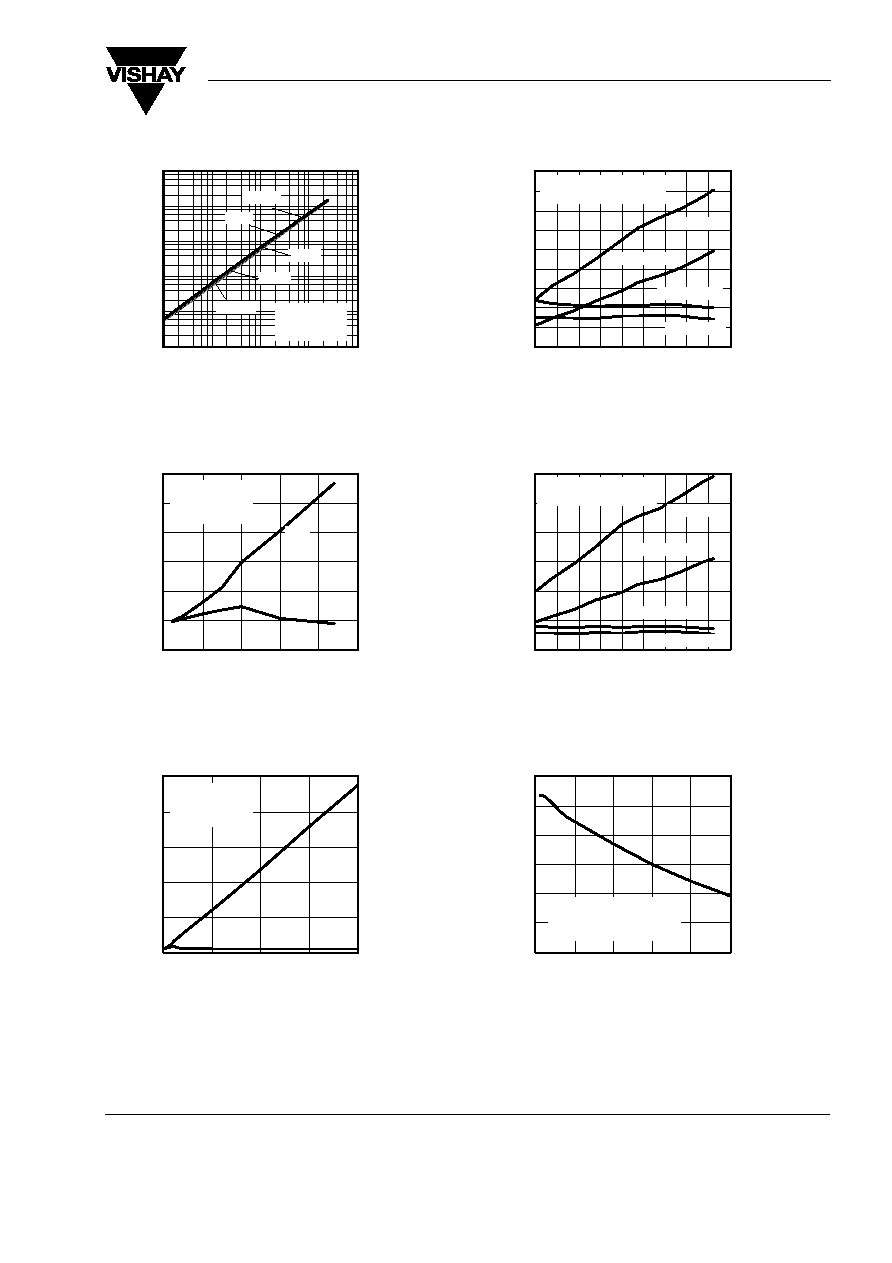
Typical Characteristics (Tamb = 25
�C unless otherwise specified)
Figure 3. Forward Voltage vs. Forward Current
Figure 4. Collector Current vs. Collector Emitter Voltage
Figure 5. Collector Current vs. Collector Emitter Voltage
0.7
0.9
1.1
1.3
1.5
1.7
1.9
2.1
2.3
0.01
0.10
1.00
10.00
100.00
I
F
� Forward Current ( mA )
17585
V � Forward V
oltage ( V )
F
110
�C
0
�C
50
�C
25
�C
�55
�C
0
1
2
3
4
5
6
7
8
9
10
11
12
0 1 2 3 4 5 6 7 8 9 10 11 12 13 14 15
V
CE
� Collector Emitter Voltage ( V )
17586
I � Collector Current ( mA
)
T
amb
= 25
_C,
V
CC
= 5 V, non�saturated
C
I
F
= 25 mA
20 mA
15 mA
10 mA
5 mA
0
1
2
3
4
5
6
7
8
0.0
0.1
0.2
0.3
0.4
0.5
V
CE
� Collector Emitter Voltage ( V )
17629
I � Collector Current ( mA
)
T
amb
= 25
_C,
V
CC
= 5 V,
saturated
C
I
F
= 25 mA
20 mA
15 mA
10 mA
5 mA
1 mA
Figure 6. Collector-Emitter Dark Current vs. Ambient Temperature
Figure 7. Normalized Current Transfer Ratio vs. Ambient
Temperature
Figure 8. Normalized Current Transfer Ratio vs. Ambient
Temperature
�55 �35 �15
5
25
45
65
85 105 125
I � Collector Emitter Leakage Current (nA)
T
amb
� Ambient Temperature (
_C )
17590
CE0
100
10
0.1
0.01
1000
V
CC
= V
CE
= 15 V
1
V
CC
= V
CE
= 5 V
0.0
0.2
0.4
0.6
0.8
1.0
1.2
1.4
1.6
1.8
2.0
�55 �35 �15
5
25
45
65
85 105 125
T
amb
� Ambient Temperature (
�C )
17630
CTR � Normalized CTR
Normalized to I
F
= 10 mA,
T
amb
= 25
_C, V
CC
= 5 V
V
O
= 0.4 V, saturated
Norm
10 mA
5 mA
I
F
= 1 mA
0.00
0.25
0.50
0.75
1.00
1.25
1.50
1.75
2.00
2.25
2.50
�55 �35 �15
5
25
45
65
85 105 125
T
amb
� Ambient Temperature (
�C )
17631
CTR � Normalized CTR
Normalized to I
F
= 16 mA,
T
amb
= 25
_C, V
CC
= 5 V
V
O
= 0.4 V, saturated
Norm
10 mA
5 mA
I
F
= 1 mA
16 mA

www.vishay.com
6
Document Number 83909
Rev. 1.5, 26-Oct-04
6N1135/ 6N1136
Vishay Semiconductors
Figure 9. Output Current vs. Temperature
Figure 10. Normalized Current Transfer Ratio vs. Ambient
Temperature
Figure 11. Normalized Current Transfer Ratio vs. Ambient
Temperature
0
1
2
3
4
5
6
7
�55 �35 �15
5
25
45
65
85 105 125
T
amb
� Ambient Temperature (
�C )
17587
I � Collector Current ( mA
)
V
CC
= 5 V,
V
O
= 0.4 V, saturated
C
I
F
= 20 mA
16 mA
10 mA
2 mA
1 mA
0.0
0.2
0.4
0.6
0.8
1.0
1.2
1.4
1.6
1.8
2.0
�55 �35 �15
5
25
45
65
85 105 125
T
amb
� Ambient Temperature (
�C )
17632
CTR � Normalized CTR
Normalized to I
F
= 10 mA,
T
amb
= 25
_C, V
CC
= 5 V
V
O
= 5 V, non�saturated
Norm
10 mA
5 mA
I
F
= 1 mA
0.0
0.2
0.4
0.6
0.8
1.0
1.2
1.4
1.6
1.8
2.0
�55 �35 �15
5
25
45
65
85 105 125
T
amb
� Ambient Temperature (
�C )
17633
CTR � Normalized CTR
Normalized to I
F
= 16 mA,
T
amb
= 25
_C, V
CC
= 5 V
V
O
= 5 V, non�saturated
Norm
10 mA
5 mA
I
F
= 1 mA
16 mA
Figure 12. Normalized HFE vs. Base Current
Figure 13. Normalized HFE vs. Base Current
Figure 14. Photo Current vs. Forward Current
0.5
0.6
0.7
0.8
0.9
1.0
1.1
1.2
1.3
1.4
0.10
1.00
10.00
100.00
I
B
� Base Current ( mA )
17634
Normalized h
FE
Normalized to
I
B
= 20
�A, T
amb
= 25
_C,
V
O
= 5 V, non saturated
110
�C
0
�C
50
�C
25
�C
�55
�C
0.0
0.2
0.4
0.6
0.8
1.0
1.2
1.4
1.6
1.8
2.0
0.10
1.00
10.00
100.00
I
B
� Base Current ( mA )
17635
Normalized h
FE
Normalized to
I
B
= 20
�A, T
amb
= 25
_C,
V
O
= 0.4 V, saturated
110
�C
0
�C
50
�C
25
�C
�55
�C
0.01
0.10
1.00
10.00
100.00
0.01
0.10
1.00
10.00
100.00
I
F
� Forward Current ( mA )
17636
I � Photo Current (
A
)
110
�C
50
�C
25
�C
0
�C
�55
�C
V
CC
= 5 V
p
m
6N1135/ 6N1136
Document Number 83909
Rev. 1.5, 26-Oct-04
Vishay Semiconductors
www.vishay.com
7
Figure 15. Photo Current vs. Forward Current
Figure 16. Switching Time vs. Load Resistance
Figure 17. Switching Time vs. Load Resistance
0.01
0.10
1.00
10.00
100.00
I
F
� Forward Current ( mA )
17637
Norm. Photo Current
110
�C
50
�C
25
�C
0
�C
�55
�C
V
CC
= 5 V
normalized to
I
F
= 16 mA
0.0001
0.001
0.01
0.1
1
10
0
500
1000
1500
2000
2500
3000
0.0
0.5
1.0
1.5
2.0
2.5
R
L
� Load Resistance ( k
)
17638
t � Switching
T
ime ( ns )
V
CC
= V
O
= 5 V,
I
F
= 16 mA
T
amb
= 25
�C
t
off
t
on
0
5000
10000
15000
20000
25000
0
5
10
15
20
R
L
� Load Resistance ( k
)
17639
t � Switching
T
ime ( ns )
V
CC
= V
O
= 5 V,
I
F
= 16 mA
T
amb
= 25
�C
t
off
t
on
Figure 18. Propagation Delay vs. Ambient Temperature
Figure 19. Propagation Delay vs. Ambient Temperature
Figure 20. Small Signal CTR vs. Forward Current
0
200
400
600
800
1000
1200
1400
1600
1800
�55 �35 �15
5
25
45
65
85 105 125
T
amb
� Ambient Temperature (
�C )
17588
t � Propagation Delay time ( ns )
V
CC
= 5 V, I
F
= 16 mA
R
L
= 1.9 k
, T
amb
= 25
�C
P
t
PLH
( 3V )
t
PHL
( 3V )
t
PHL
( 1.5V )
t
PLH
( 1.5V )
0
500
1000
1500
2000
2500
3000
�55 �35 �15
5
25
45
65
85 105 125
T
amb
� Ambient Temperature (
�C )
17589
t � Propagation Delay time ( ns )
T
amb
= 25
�C, V
CC
= 5 V,
I
F
= 16 mA, R
L
= 4.1 k
P
t
PLH
( 3V )
t
PHL
( 3V )
t
PHL
( 1.5V )
t
PLH
( 1.5V )
0.0
0.1
0.2
0.3
0.4
0.5
0.6
0
5
10
15
20
25
I
F
� Forward Current ( mA )
17591
Small Signal Current
T
ransfer Ratio
V
CC
= V
O
= 5 V,
R
L
= 100
, R
LED
= 50
,
T
amb
= 25
_C
www.vishay.com
8
Document Number 83909
Rev. 1.5, 26-Oct-04
6N1135/ 6N1136
Vishay Semiconductors
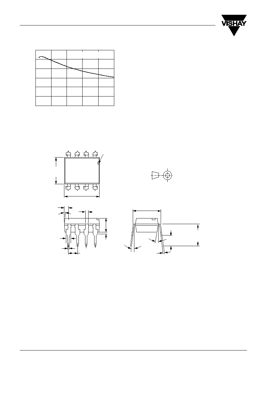
Package Dimensions in Inches (mm)
i6n135_11
0.6
0.5
0.4
0.3
0.2
0.1
0
10
15
20
25
i
F
/
i
O
/
Small
Signal
Current
Transfer
Ratio
IF / mA
5
0
(VCC = 5.0 V, RL = 100 )
Figure 21. Small Signal Current Transfer Ratio vs. Quiescent Input
Current
i178006
pin one ID
.255 (6.48)
.268 (6.81)
.379 (9.63)
.390 (9.91)
.030 (0.76)
.045 (1.14)
4� typ.
.100 (2.54) typ.
10�
3��9�
.300 (7.62)
typ.
.018 (.46)
.022 (.56)
.008 (.20)
.012 (.30)
.110 (2.79)
.130 (3.30)
.130 (3.30)
.150 (3.81)
.020 (.51 )
.035 (.89 )
.230(5.84)
.250(6.35)
4
3
2
1
.031 (0.79)
.050 (1.27)
5
6
7
8
ISO Method A
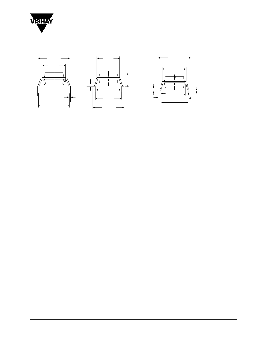
6N1135/ 6N1136
Document Number 83909
Rev. 1.5, 26-Oct-04
Vishay Semiconductors
www.vishay.com
9
min.
.315 (8.00)
.020 (.51)
.040 (1.02)
.300 (7.62)
ref.
.375 (9.53)
.395 (10.03)
.012 (.30) typ.
.0040 (.102)
.0098 (.249)
15� max.
Option 9
.014 (0.35)
.010 (0.25)
.400 (10.16)
.430 (10.92)
.307 (7.8)
.291 (7.4)
.407 (10.36)
.391 (9.96)
Option 6
.315 (8.0)
MIN.
.300 (7.62)
TYP.
.180 (4.6)
.160 (4.1)
.331 (8.4)
MIN.
.406 (10.3)
MAX.
.028 (0.7)
MIN.
Option 7
18450

www.vishay.com
10
Document Number 83909
Rev. 1.5, 26-Oct-04
6N1135/ 6N1136
Vishay Semiconductors
Ozone Depleting Substances Policy Statement
It is the policy of Vishay Semiconductor GmbH to
1. Meet all present and future national and international statutory requirements.
2. Regularly and continuously improve the performance of our products, processes, distribution and
operatingsystems with respect to their impact on the health and safety of our employees and the public, as
well as their impact on the environment.
It is particular concern to control or eliminate releases of those substances into the atmosphere which are
known as ozone depleting substances (ODSs).
The Montreal Protocol (1987) and its London Amendments (1990) intend to severely restrict the use of ODSs
and forbid their use within the next ten years. Various national and international initiatives are pressing for an
earlier ban on these substances.
Vishay Semiconductor GmbH has been able to use its policy of continuous improvements to eliminate the use
of ODSs listed in the following documents.
1. Annex A, B and list of transitional substances of the Montreal Protocol and the London Amendments
respectively
2. Class I and II ozone depleting substances in the Clean Air Act Amendments of 1990 by the Environmental
Protection Agency (EPA) in the USA
3. Council Decision 88/540/EEC and 91/690/EEC Annex A, B and C (transitional substances) respectively.
Vishay Semiconductor GmbH can certify that our semiconductors are not manufactured with ozone depleting
substances and do not contain such substances.
We reserve the right to make changes to improve technical design
and may do so without further notice.
Parameters can vary in different applications. All operating parameters must be validated for each
customer application by the customer. Should the buyer use Vishay Semiconductors products for any
unintended or unauthorized application, the buyer shall indemnify Vishay Semiconductors against all
claims, costs, damages, and expenses, arising out of, directly or indirectly, any claim of personal
damage, injury or death associated with such unintended or unauthorized use.
Vishay Semiconductor GmbH, P.O.B. 3535, D-74025 Heilbronn, Germany
Telephone: 49 (0)7131 67 2831, Fax number: 49 (0)7131 67 2423