 | –≠–ª–µ–∫—Ç—Ä–æ–Ω–Ω—ã–π –∫–æ–º–ø–æ–Ω–µ–Ω—Ç: 71117 | –°–∫–∞—á–∞—Ç—å:  PDF PDF  ZIP ZIP |

Si9113DB
Vishay Siliconix
Document Number: 71117
29-Feb-00
www.siliconix.com
S
FaxBack 408-970-5600
1
Si9113 Demonstration Board
FEATURES
D
ISDN-NT Input Voltage Range 28 V to 99 V
D
Non-Polar Input
D
3.3-V/120-mA, 40-V/12-mA Outputs With Up To 80% Efficiency
D
Up to 68% Efficiency at 80-mW Load
D
40 V Isolated By 3 kV From Input And 3.3-V Output ≠ Si9113D1
D
3.3 V, 40 V Isolated By 1.5 kV From Input/Each Other ≠ Si9113D2
D
Current Mode Control, 0.6-V Fast Over-Current Protection
D
Max 50% Duty Cycle Operation
D
1.3-MHz Error Amp
D
Soft-Start
D
<10-
m
A Supply Current for +V
IN
<18 V
D
Programmed Start/Stop
D
Internal Start-Up Circuit
D
Power_Good Output
DESCRIPTION
As discussed in application note, AN728, the Si9113 power
supply controller is an ideal choice for ISDN terminal
equipment, where high efficiency at a low power level is one of
most important criteria. Therefore, Vishay Siliconix has
developed versions of a dual output flyback application
demonstration boards, the Si9113D1 and the Si9113D2, which
use different regulation schemes. These readily available
demo boards are configured to deliver approximately 800 mW
at 3.3-V, and40-V. These outputs and can be easily modified
for other output voltages at approximately same power level.
The flyback converters are designed to operate from a wide
input voltage range of 28 V to 99 V and are polarity protected
by a diode bridge. The Si9113D1 and Si9113D2, both operate
at 20-kHz switching frequency to achieve the best possible
efficiency. The transformer is selected to be slightly larger in
this application so that the same area product would be good
enough for an even lower window utilization factor (w.u.f.)
transformer in order to meet the stringent requirements of
clearance and creepage distances.
The Si9113D1 senses and tightly regulates the main output
V
OUT1
(3.3 V), which has the common ground as input and the
secondary output V
OUT2
(40 V) is regulated to within
$
10% at
10% to100% load range, including the set point accuracy.
Correspondingly. the transformer must be specified with tight
tolerance to achieve the given set point accuracy. The 40-V
output is isolated from both the input and 3.3-V output by
minimum 3 kV
rms
isolation.
The Si9113D2 uses the auxiliary output (V
CC
bootstrap
winding) for sensing. Both V
OUT1
(3.3 V) and V
OUT2
(40 V)
follow the auxiliary output, residing on one core and sharing the
same flux. Both the outputs are isolated from the input as well
as from each other by 1.5 kV and moderately regulated to
$
5%.
Each demonstration board uses all surface mount
components except the high voltage electrolyte capacitor and
are fully assembled and tested for quick evaluation. Test points
are provided for the power_good signal and the closed loop
response measurement.
Included in this document are the Bill-Of-Materials,
Schematics, PCB Layout of the Demo Boards and actual
waveforms/graphs.
The demonstration board layout is available in Gerber file format. Please contact your Vishay Siliconix sales representative or
distributor for a copy.
ORDERING INFORMATION:
Si9113D1-- V
OUT1
(3.3 V) Tightly regulated, non-isolated
V
OUT2
(40 V) Loosely regulated, 3 kV isolated
Si9113D2-- V
OUT1
(3.3 V) Moderately regulated, 1.5 kV isolated
V
OUT2
(40 V) Moderately regulated, 1.5 kV isolated
Si9113DB
Vishay Siliconix
www.Vishay Siliconix.com
S
FaxBack 408-970-5600
2
Document Number: 71117
29-Feb-00
POWER UP CHECK LIST AND OPERATION
The Si9113D1 and Si9113D2 are designed to operate in
discontinuous mode at nominal line and load conditions. Both
demo boards use the same operational procedure, as follows:
1
Visually inspect the PCB to be sure that all the components
are intact and no foreign substance is lying on the board.
2
Solder the leads at C1 negative and MOSFET Q1 drain to
monitor the drain waveform on the oscilloscope.
3
Reduce the source voltage to zero and connect it through
the dc ammeter at V
IN
+ and V
IN
≠. Connect the dc
voltmeter precisely across V
IN
+ and V
IN
≠. For the
application where input is of fixed polarity, the diode bridge
BR1 can be eliminated by shorting pin 1 to 4 and pin 2 to
3 to achieve even higher efficiency.
4
Connect the voltmeter precisely across V
OUT1
≠ Com1 and
V
OUT2
≠ Com2 for the output voltage measurement.
Connect the oscilloscope ground to C1 negative while the
probe to Q1 drain to observe the switching waveforms.
5
Slowly increase the input voltage while monitoring the input
current meter. Note the input current is less than 10
m
A at
18 V
IN
and continue to increase the voltage further till the
circuit turns on at approximately 24 V.
6
Set the input voltage to 48 V nominal and monitor the drain
waveform, switching frequency, input and output ripple and
noise.
7
The efficiency, line, load and cross regulation can be
measured by varing the line between 28 to 99 V, and the
load between 10% and 100%.
ACTUAL WAVEFORMS AND PERFORMANCE
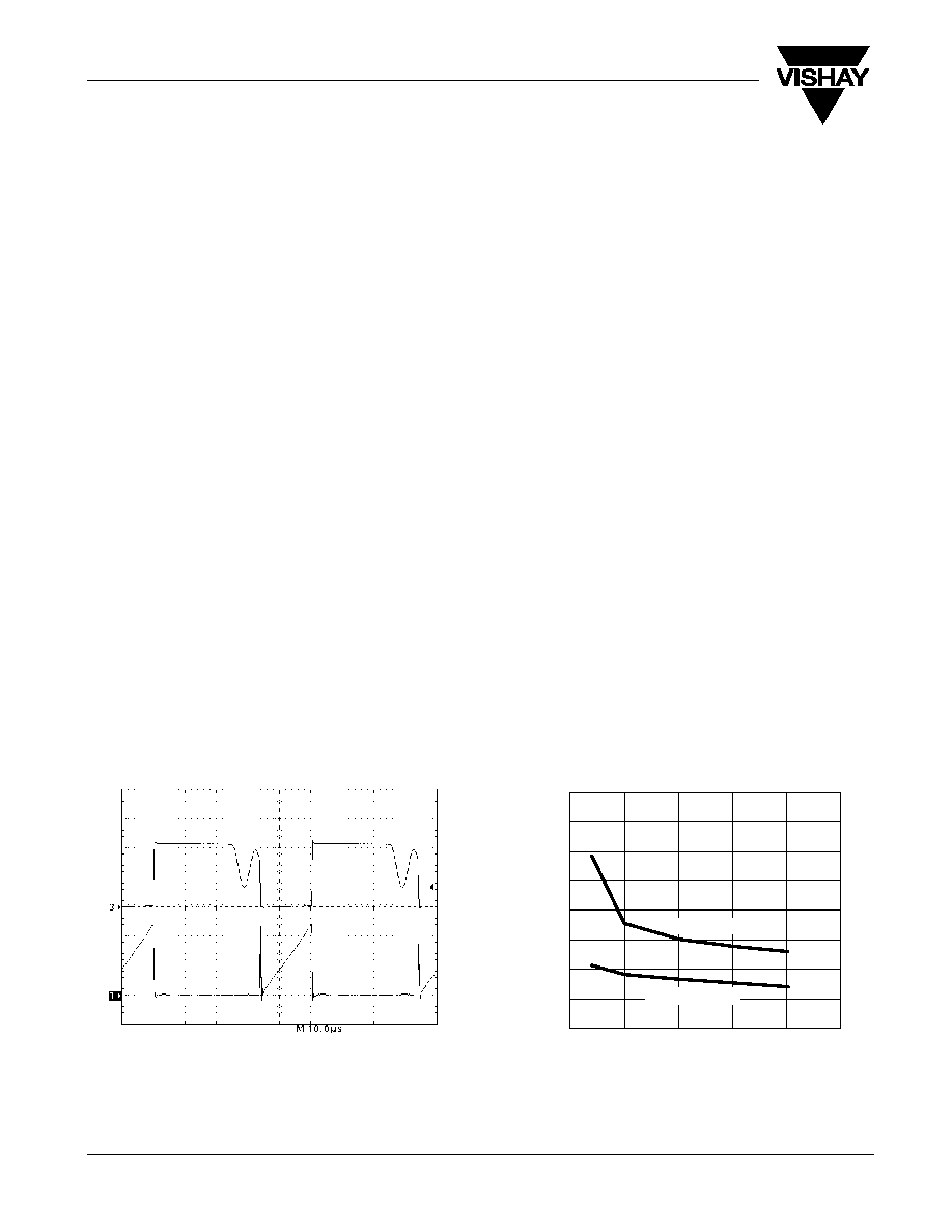
Drain Voltage and Current
The circuit is designed to operate in discontinuous mode at
nominal line and full load. The transformer is cleverly designed
to reduce the leakage inductance. Refer to Figure 1 for the
drain voltage and current waveforms. The current starting from
zero indicates the discontinuous mode operation and absence
of any leakage spike at drain shows the tight coupling between
the windings.
V
IN
= 28 V
Outputs ≠ Full lLoad
Ch1 ≠ Primary Current (0.1A/div)
Ch3 ≠ Drain Voltage (20 V/div)
FIGURE 1. Drain Voltage and Current Waveform ≠ Si9113D2
36.00
37.00
38.00
39.00
40.00
41.00
42.00
43.00
44.00
0
3.00
6.00
9.00
12.00
15.00
FIGURE 2. V
OUT2
(40 V) Load/cross Regulation ≠ Si9113D1
(V)
3.3 V @ 12 mA
3.3 V @ 120 mA
V
OUT2
I
OUT2
(mA)

Si9113DB
Vishay Siliconix
Document Number: 71117
29-Feb-00
www.siliconix.com
S
FaxBack 408-970-5600
3
Output Regulation
The output regulation of slave outputs depend upon the
loading condition of main output.
In Si9113D1, the V
OUT1
(3.3 V) is tightly regulated to within 1%,
while V
OUT2
(40 V) follows the main output. Figure 2 depicts
the typical load regulation of 40 V output, when the main output
is at 10% and at full load condition.
In Si9113D2, the V
OUT1
and V
OUT2
are both moderately
regulated. Figures 3 and 4 show the 3.3-V and 40-V regulation
with the outputs loaded at 10% to100% of the rated load. The
output voltages are essentially constant with respect to any
variation of input voltage in case of both demo boards.
Output Ripple and Noise
The tantalum chip capacitors are used for lower ESR and
higher ripple current capability. Low cost aluminium capacitors
can also be used where form fator and/or output ripple are of
secondary importance. Also, a small additional LC filter can be
added at 3.3-V output for further attenuation of ac component
by even five to ten times. The Si9113D1 ≠ Figure 5 and
Si9113D2 ≠ Figure 6 show the ripple at a full load and 48-V
input.
(V)
3.140
3.180
3.220
3.260
3.300
3.340
3.380
3.420
3.460
0
25
50
75
100
125
150
FIGURE 3. V
OUT1
(3.3 V) Load/cross Regulation ≠ Si9113D2
40 V @ 1.2 mA
40 V @ 12 mA
V
OUT1
I
OUT1
(mA)
38.00
38.50
39.00
39.50
40.00
40.50
41.00
41.50
42.00
0
3.00
6.00
9.00
12.00
15.00
FIGURE 4. V
OUT2
(40 V) Load/Cross Regulation ≠ Si9113D2
3.3 V @ 12 mA
I
OUT2
(mA)
V
out2 (V)
3.3 V @ 120 mA
V
IN
= 48 V
Outputs = At Full Load
Ch1 = 3.3 V (20 mV/div))
Ch3 = 40 V (100 mV/div)
FIGURE 5. Output Ripple and Noise ≠ Si9113D1
V
IN
= 48 V
Outputs = At Full Load
Ch1 = 3.3 V (20 mV/div))
Ch3 = 40 V (100 mV/div)
FIGURE 6. Output Ripple and Noise ≠ Si9113D2

Si9113DB
Vishay Siliconix
www.Vishay Siliconix.com
S
FaxBack 408-970-5600
4
Document Number: 71117
29-Feb-00
EFFICIENCY
0.00
10.00
20.00
30.00
40.00
50.00
60.00
70.00
80.00
90.00
0
200
400
600
800
1000
FIGURE 7. Converter Output Load vs Efficiency ≠ Si9113D1
V
IN
= 99 V
W
O
(mW)
Ef
ficiency %
V
IN
= 48 V
V
IN
= 28 V
0.00
10.00
20.00
30.00
40.00
50.00
60.00
70.00
80.00
90.00
0
200
400
600
800
1000
FIGURE 8. Converter Output Load vs Efficiency ≠ Si9113D2
V
IN
= 99 V
W
O
(mW)
Ef
ficiency %
V
IN
= 48 V
V
IN
= 28 V
COMPENSATION
The closed loop response is observed at 48 V
IN
and full load
at both outputs on the venable by applying the error across R8
and measuring the gain, phase change encountered by the
signal at both ends of R8. Refer to Figures 9 and 10 for the
actual response.
FIGURE 9. Measured Close Loop Response ≠ Si9113D1
≠180
≠150
≠120
≠90
≠60
≠30
0
30
60
90
120
150
180
≠60
≠50
≠40
≠30
≠20
≠10
0
10
20
30
40
50
60
Gain (dB)
Frequency (Hz)
Phase
10
100
1,000
10,000
50,000
Phase
Gain
≠80
≠60
≠40
≠20
0
20
40
60
80
10
100
1000
10000
≠120
≠90
≠60
≠30
0
30
60
90
120
≠80
≠60
≠40
≠20
0
20
40
60
80
10
100
1000
10000
≠120
≠90
≠60
≠30
0
30
60
90
120
FIGURE 10. Measured Closed Loop Response≠Si9113D2
Phase
Gain
Frequency (Hz)
Phase
Gain
Phase
Gain (dB)

Si9113DB
Vishay Siliconix
Document Number: 71117
29-Feb-00
www.siliconix.com
S
FaxBack 408-970-5600
5
Dynamic Load Response
The step load is applied at 1A/
m
S slew rate at one output, while keeping the other output at rated load. Refer to Figures 11 through 14.
FIGURE 11. V
OUT1
(3.3 V) Transient Load Response ≠ Si9113D1
V
IN
= 48 V
V
OUT1
= Step ≠12 to 120 mA
Ch1 = V
OUT1
(3.3 V)
Ch4 = Load (50 mA/div)
Slew Rate = 1A/
m
sec
V
IN
= 48 V
V
OUT2
= Step Load 1.2 to 12 mA
V
OUT1
= At Full Load
Ch1 = V
OUT2
(40 V)
Ch4 = Load (10 mA/div)
Slew Rate = 1A/
m
sec
FIGURE 12. V
OUT2
(40 V) Transient Load Response ≠ Si9113D1
V
IN
= 48 V
V
OUT1
= Step Load 12 mA ≠ 120 mA
V
OUT2
= At Full Load
Ch1 = V
OUT1
(3.3 V)
Ch4 = 100 mA/div
Slew Rate = 1A/
m
sec
FIGURE 13. V
OUT1
(3.3 V) Transient Load Response--Si9113D2
V
IN
= 48 V
V
OUT2
= Step Load 1.2 mA ≠ 12 mA
V
OUT1
= At Full Load
Ch1 = V
OUT2
(40 V)
Ch4 = 10 mA/div
Slew Rate = 1A/
m
sec
FIGURE 14. V
OUT2
(40 V) Transient Load Response--Si9113D2

Si9113DB
Vishay Siliconix
www.Vishay Siliconix.com
S
FaxBack 408-970-5600
6
Document Number: 71117
29-Feb-00
SCHEMATIC, PCB LAYOUT AND BILL OF MATERIAL (SI9113D1)
C3
220 pF
OSC
IN
OSC
OUT
SS
V
REF
FB
COMP
START
V
CC
DR
GND
PWR_G
ICS
V
IN
STOP
Si9113
7
6
5
4
2
1
3
8
9
10
11
13
14
12
R5
3.96 M
W
R4
1 M
W
R2
300 k
W
C8
0.01
m
F
C13
100 pF
C6
0.1
m
F
C7
0.001
m
F
R1
1 M
W
R3
5.1 M
W
R10
13 k
W
R9
20 k
W
R8
51
W
C5
0.1
m
F
TP1
PWR_GD
C9
0.01
m
F
R6
5.1
W
R11
1 k
W
R7
2
W
1
/
2
W
C12
0.1
m
F
D2
ESIG
NS2
C10
2.2
m
F
50 V
D4*
BZX84C43
P3
40 V
P6
COM
2
C10
2.2
m
F
50 V
D3
B130LB
R12
5.1 k
W
(NU)
P5
COM
1
P3
3.3 V
R13
2.7
W
D1
ESIG
2, 4 (Q1)
1, 2, 5, 6, (Q01)
Q1
BSP89 (NU)
Q01
Si3420DV
3 (Q1)
4 (Q01)
TP2
NP
7
9
8
NS3
1
3
3
1
+
C2
0.1
m
F
160 V
(NU)
T1
XFMR_LPE9080
C4
1
m
F
D5*
BZX84C15
3
1
C1
22
m
F
160 V
AC
AC
+
≠
2
1
3
4
P1
V
IN
P2
GND
6
5
BR1
DF02S
*Optional
+
1 (Q1)
3 (Q01)
FIGURE 15. Demo Board--Si9113D1
Dual Output Flyback Converter with Tightly Regulated Main Output

Si9113DB
Vishay Siliconix
Document Number: 71117
29-Feb-00
www.siliconix.com
S
FaxBack 408-970-5600
7
FIGURE 16. Silk Screen--Si9113D1
FIGURE 17. Top Layer--Si9113D1
FIGURE 18. Bottom Layer--Si9113D1

Si9113DB
Vishay Siliconix
www.Vishay Siliconix.com
S
FaxBack 408-970-5600
8
Document Number: 71117
29-Feb-00
TABLE 1. BILL OF MATERIALS Si9113D1
Item
Qty
Designator
Part Type
Description
Footprint
Vendor Part #
Manufacturer
1
2
"R1, R4"
1 M
W
"RES, 1%,
1
/
8
W"
0805
CRCW08051004FRT1
Vishay Dale
2
1
R2
300 k
W
"RES, 1%,
1
/
8
W"
0805
CRCW08053003FRT1
Vishay Dale
3
1
R3
5.1 M
W
"RES, 1%,
1
/
8
W"
0805
CRCW08055104FRT1
Vishay Dale
4
1
R5
3.96 M
W
RES, 1%,
1
/
8
W"
0805
CRCW08053964FRT1
Vishay Dale
5
1
R6
5.1
W
RES, 5%,
1
/
8
W"
0805
CRCW080551JRT1
Vishay Dale
6
1
R7
2
W
"RES, 1%,
1
/
2
W, PWR Metal"
2010
WSC-
1
/
2
Vishay Dale
7
1
R8
51
W
"RES, 5%,
1
/
8
W"
0805
CRCW0805510JRT1
Vishay Dale
8
1
R9
20 k
W
"RES, 1%,
1
/
8
W"
0805
CRCW08052002FRT1
Vishay Dale
9
1
R10
13 k
W
"RES, 1%,
1
/
8
W"
0805
CRCW08051302FRT1
Vishay Dale
10
1
R11
1 k
W
"RES, 1%,
1
/
8
W"
0805
CRCW08051001FRT1
Vishay Dale
11
1
R12 (NU)
5.1 k
W
"RES, 1%,
1
/
8
W (NU)"
0805
CRCW08055101FRT1
Vishay Dale
12
1
R13
2.7
W
"RES, 5%,
1
/
8
W"
0805
CRCW080527JRT1
Vishay Dale
13
1
C1
22
m
F
"CAP, ELEC, 160 V, VR "
RB.2/.4
UVR2C220MEA
Nichicon
14
1
C2 (NU)
0.1
m
F
"CAP, CER, 200 V"
1206
VJ1210Y104KXC
Vishay Vitramon
15
1
C3
220 pF
"CAP, CER"
0805
VJ0805Y221KXXAT
Vishay Vitramon
16
1
C4
1
m
F
"CAP, CER, 25 V"
1210
VJ1210U105ZXAA
Vishay Vitramon
17
3
"C5, C6, C12"
0.1
m
F
"CAP, CER"
0805
VJ0805Y104KXXAT
Vishay Vitramon
18
1
C7
0.001
m
F
"CAP, CER"
0805
VJ0805Y102KXXAT
Vishay Vitramon
19
2
"C8, C9"
0.01
m
F
"CAP, CER"
0805
VJ0805Y103KXXAT
Vishay Vitramon
20
1
C10
2.2
m
F
"CAP, TAN, 50 V"
595D_C
595D225X0050C2T
Vishay Sprague
21
1
C11
220
m
F
"CAP, TAN, 6.3 V"
594D_C
594D227X06R3C2T
Vishay Sprague
22
1
C13
100 pF
"CAP, CER"
0805
VJ0805Y101KXXAT
Vishay Vitramon
23
2
"D1, D2"
ES1G
"Diode, 1 A"
SMA
ES1G
Vishay Liteon
24
1
D3
B130LB
"Schottky Diode, 1 A"
SMB
B130LB
Vishay Liteon
25
1
D4*
BZX84C43
"Zener Diode, 41 V"
SOT-23
BZX84C43
Vishay Liteon
26
1
D5
BZX84C15
Zener Diode
SOT-23
BZX84C15
Vishay Dale
27
1
T1
LPE-9080-A413
Transformer
XFMR_LPE9080
LPE-9080-A413
Vishay Liteon
28
1
BR1
DF04S
Bridge
BR1
Vishay Liteon
29
1
Q1 (NU)
BSP89
N≠Channel DMOSFET (NU)
SOT-223
BSP89
Philips Semiconductors
30
1
Q01
Si3420DV
N≠Channel MOSFET
TSOP-6
Si3420DV
Vishay Siliconix
31
1
U1
Si9113
Power IC
SO≠14
Si9113
Vishay Siliconix
32
2
"TP1, TP2"
Test Point
1-Pin Header
TP1
Multi-Source
33
6
P1 TO P6
"PWR, GND"
1-Pin Header
TP1
Multi-Source
*Optional

Si9113DB
Vishay Siliconix
Document Number: 71117
29-Feb-00
www.siliconix.com
S
FaxBack 408-970-5600
9
SCHEMATIC, PCB LAYOUT AND BILL OF MATERIAL (SI9113D2)
P4
3.3 V
C3
470 pF
OSC
IN
OSC
OUT
SS
V
REF
FB
COMP
START
V
CC
DR
GND
PWR_G
ICS
V
IN
STOP
Si9113
7
6
5
4
2
1
3
8
9
10
11
13
14
12
R5
3.96 M
W
R4
1 M
W
R2
300 k
W
C8
0.01
m
F
C2
100 pF
C6
0.1
m
F
C7
0.001
m
F
R1
1 M
W
R3
5.1 M
W
C5
0.1
m
F
TP1
PWR_GD
C9
0.01
m
F
R6
5.1
W
R11
1 k
W
R7
2
W
1
/
2
W
D2
ESIG
NS2
C10
2.2
m
F
50 V
D4*
BZX84C43
P3
40 V
P6C
OM
2
R13
2.7
W
D1
ESIG
1, 2, 5, 6, (Q01)
2, 4 (Q1)
Q1
BSP89(NU)
Q01
Si3420DV
3 (Q1)
4 (Q01)
NP
8
7
6
NS3
4
3
3
1
+
T1
LPE9080
C1
22
m
F
160 V
AC
AC
+
≠
2
1
3
4
P1
V
IN
P2
GND
5
9
BR1
DF02S
*Optional
+
3 (Q01)
1 (Q1)
FIGURE 19. Demo Board--Si9113D2
D3
B130LB
NS1
C11
220
m
F
10 V
P5
COM
1
2
1
+
R12
5.1 k
W
(NU)
C12
0.1
m
F
C4
1
m
F
R10
12.7 k
W
R8
51
W
R9
89 k
W
TP2
Dual Output Flyback Converter with Moderately Regulated Outputs

Si9113DB
Vishay Siliconix
www.Vishay Siliconix.com
S
FaxBack 408-970-5600
10
Document Number: 71117
29-Feb-00
FIGURE 20. Silk Screen--Si9113D2
FIGURE 21. Top Layer--Si9113D2
FIGURE 22. Bottom Layer--Si9113D2

Si9113DB
Vishay Siliconix
Document Number: 71117
29-Feb-00
www.siliconix.com
S
FaxBack 408-970-5600
11
TABLE 2. BILL OF MATERIALS Si9113D2
Item
Qty
Designator
Part Type
Description
Footprint
Vendor Part #
Manufacturer
1
2
"R1, R4"
1 M
W
"RES, 1%,
1
/
8
W"
0805
CRCW08051004FRT1
Vishay Dale
2
1
R2
300 k
W
"RES, 1%,
1
/
8
W"
0805
CRCW08053003FRT1
Vishay Dale
3
1
R3
5.1 M
W
"RES, 1%,
1
/
8
W"
0805
CRCW08055104FRT1
Vishay Dale
4
1
R5
3.96 M
W
"RES, 1%,
1
/
8
W"
0805
CRCW08053964FRT1
Vishay Dale
5
1
R6
5.1
W
"RES, 5%,
1
/
8
W"
0805
CRCW080551JRT1
Vishay Dale
6
1
R7
2
W
"RES, 1%,
1
/
2
W, PWR Metal"
2010
WSC-
1
/
2
Vishay Dale
7
1
R8
51
W
"RES, 5%,
1
/
8
W"
0805
CRCW0805510JRT1
Vishay Dale
8
1
R9
89 k
W
"RES, 1%,
1
/
8
W"
0805
CRCW08058902FRT1
Vishay Dale
9
1
R10
12.7 k
W
"RES, 1%,
1
/
8
W"
0805
CRCW08051272FRT1
Vishay Dale
10
1
R11
1 k
W
"RES, 1%,
1
/
8
W"
0805
CRCW08051001FRT1
Vishay Dale
11
1
R12
5.1 k
W
"RES, 1%,
1
/
8
W"
0805
CRCW08055101FRT1
Vishay Dale
12
1
R13
2.7
W
"RES, 5%,
1
/
8
W"
0805
CRCW080527JRT1
Vishay Dale
13
1
C1
22
m
F
"CAP, ELEC, 160 V, VR"
RB.2/.4
UVR2C220MEA
Nichicon
14
1
C2
100 pF
"CAP, CER"
0805
VJ0805Y101KXXAT
Vishay Vitramon
15
1
C3
470 pF
"CAP, CER"
0805
VJ0805Y471KXXAT
Vishay Vitramon
16
1
C4
1
m
F
"CAP, CER, 25 V"
1210
VJ1210U105ZXAA
Vishay Vitramon
17
3
"C5, C6, C12"
0.1
m
F
"CAP, CER"
0805
VJ0805Y104KXXAT
Vishay Vitramon
18
1
C7
0.001
m
F
"CAP, CER"
0805
VJ0805Y102KXXAT
Vishay Vitramon
19
2
"C8, C9"
0.01
m
F
"CAP, CER"
0805
VJ0805Y103KXXAT
Vishay Vitramon
20
1
C10
2.2
m
F
"CAP, TAN, 50 V"
595D_C
595D225X0050C2T
Vishay Sprague
21
1
C11
220
m
F
"CAP, TAN, 6.3 V"
594D_C
594D227X06R3C2T
Vishay Sprague
22
2
"D1, D2"
ES1G
"Diode, 1 A"
SMA
ES1G
Vishay Liteon
23
1
D3
B130LB
"Schottky Diode, 1 A"
SMB
B130LB
Vishay Liteon
24
1
D4*
BZX84C43
"Zener Diode, 41 V"
SOT≠23
BZX84C43
Vishay Liteon
25
1
T1
LPE-9080-A414
Transformer
XFMR_LPE908
0
LPE-9080-A414
Vishay Dale
26
1
BR1
DF04S
Bridge
BR1
Vishay Liteon
27
1
Q1 (NU)
BSP89
N≠Channel DMOSFET (NU)
SOT-223
BSP89
Philips Semicoductors
28
1
Q01
Si3420DV
N≠Channel MOSFET
TSOP-6
Si2320DS
Vishay Siliconix
29
1
U1
Si9113
Power IC
SO-14
Si9113
Vishay Siliconix
30
2
"TP1, TP2"
Test Point
1-Pin Header
TP1
Multi-Source
31
6
P1 TO P6
"PWR, GND"
1-Pin Header
TP1
Multi-Source
*Optional