 | –≠–ª–µ–∫—Ç—Ä–æ–Ω–Ω—ã–π –∫–æ–º–ø–æ–Ω–µ–Ω—Ç: 83816 | –°–∫–∞—á–∞—Ç—å:  PDF PDF  ZIP ZIP |

LH1518AAB/ AABTR/ AT
Document Number 83816
Rev. 1.3, 26-Oct-04
Vishay Semiconductors
www.vishay.com
1
4
6
5
S'
S
DC
1
2
3
S
S'
i179001
DIP
SMD
Pb
Pb-free
e3
1 Form A Solid State Relay
Features
∑ Isolation Test Voltage 5300 V
RMS
∑ Current-limit Protection
∑ High-reliability Monolithic Detector
∑ Low Power Consumption
∑ Clean, Bounce-free Switching
∑ High Surge Capability
∑ Surface Mountable
∑ Lead-free component
∑ Component in accordance to RoHS 2002/95/EC
and WEEE 2002/96/EC
Agency Approvals
∑ UL1577, File No. E52744 System Code H or J,
Double Protection
∑ CSA - Certification 093751
∑ BSI/BABT Cert. No. 7980
∑ DIN EN 60747-5-2 (VDE0884)
DIN EN 60747-5-5 pending
∑ FIMKO Approval
Applications
General Telecom Switching
Instrumentation
Industrial Controls
Description
Vishay Solid State Relays (SSRs) are miniature, opti-
cally- coupled relays with high-voltage MOSFET out-
puts. The LH1518 relays are capable of switching AC
or DC loads from as little as nanovolts to hundreds of
volts.
The relays can switch currents in the range of nano-
amps to hundreds of milliamps. The MOSFET
switches are ideal for small signal switching and are
primarily suited for dc or audio frequency applica-
tions.
The LH1518 relays feature a monolithic output die
that minimizes wire bonds and permits easy integra-
tion of high-performance circuits such as current lim-
iting in normally-open switches. The output die
integrates the photodiode receptor array, turn-on and
turn-off control circuitry, and the MOSFET switches.
The optically-coupled input is controlled by a highly
efficient GaAlAs infrared LED.
Order Information
Part
Remarks
LH1518AAB
Tubes, SMD-6
LH1518AABTR
Tape and Reel, SMD-6
LH1518AT
Tubes, DIP-6

www.vishay.com
2
Document Number 83816
Rev. 1.3, 26-Oct-04
LH1518AAB/ AABTR/ AT
Vishay Semiconductors
Absolute Maximum Ratings, T
amb
= 25 ∞C
Stresses in excess of the absolute Maximum Ratings can cause permanent damage to the device. Functional operation of the device is
not implied at these or any other conditions in excess of those given in the operational sections of this document. Exposure to absolute
Maximum Ratings for extended periods of time can adversely affect reliability.
SSR
1)
Refer to Current Limit Performance Application Note 58 for a discussion on relay operation during transient currents.
Electrical Characteristics, T
amb
= 25 ∞C
Minimum and maximum values are testing requirements. Typical values are characteristics of the device and are the result of engineering
evaluations. Typical values are for information only and are not part of the testing requirements.
Input
Output
Parameter
Test condition
Symbol
Value
Unit
LED continuous forward current
I
F
50
mA
LED reverse voltage
I
R
10 µA
V
R
8.0
V
DC or peak AC load voltage
V
L
250
V
Continuous DC load current,
bidirectional operation
I
L
155
mA
Continuous DC load current,
unidirectional operation
I
L
300
mA
Peak load current (single shot)
t = 100 ms
I
P
1)
Ambient temperature range
T
amb
- 40 to + 85
∞C
Storage temperature range
T
stg
- 40 to + 150
∞C
Pin soldering temperature
t = 10 s max
T
sld
260
∞C
Input/output isolation voltage
V
ISO
5300
V
RMS
Output power dissipation
(continuous)
P
diss
550
mW
Parameter
Test condition
Symbol
Min
Typ.
Max
Unit
LED forward current,
switch turn-on
I
L
= 100 mA, t = 10 ms
I
Fon
0.8
2.0
mA
LED forward current,
switch turn-off
V
L
= ± 200 V
I
Foff
0.2
0.7
mA
LED forward voltage
I
F
= 10 mA
V
F
1.15
1.26
1.45
V
Parameter
Test condition
Symbol
Min
Typ.
Max
Unit
ON-resistance ac/dc:
Pin 4(±) to 6 (±)
I
F
= 5.0 mA, I
L
= 50 mA
R
ON
10
15
20
ON-resistance dc:
Pin 4, 6 (+) to 5 (±)
I
F
= 5.0 mA, I
L
= 100 mA
R
ON
2.5
3.75
5.0
Off-resistance
I
F
= 0 mA, V
L
= ± 100 V
R
OFF
0.5
5000
G
Current limit ac/dc :
Pin 4 (±) to 6 (±)
I
F
= 5.0 mA, V
L
= ± 6.0 V,
t = 5.0 ms
I
LMT
170
200
280
mA
Off-state leakage current
I
F
= 0 mA, V
L
= ± 100 V
I
O
0.02
200
nA
I
F
= 0 mA, V
L
= ± 250 V
I
O
1.0
µA
Output capacitance Pin 4 to 6
I
F
= 0 mA, V
L
= 1.0 V
C
O
55
pF
I
F
= 0 mA, V
L
= 50 V
C
O
10
pF
Switch offset
I
F
= 5.0 mA
V
OS
0.15
V

LH1518AAB/ AABTR/ AT
Document Number 83816
Rev. 1.3, 26-Oct-04
Vishay Semiconductors
www.vishay.com
3
Transfer
Typical Characteristics (Tamb = 25
∞C unless otherwise specified)
Parameter
Test condition
Symbol
Min
Typ.
Max
Unit
Capacitance (input-output)
V
ISO
= 1.0 V
C
IO
0.8
pF
Turn-on time
I
F
= 5.0 mA, I
L
= 50 mA
t
on
1.4
3.0
ms
Turn-off time
I
F
= 5.0 mA, I
L
= 50 mA
t
off
0.7
3.0
ms
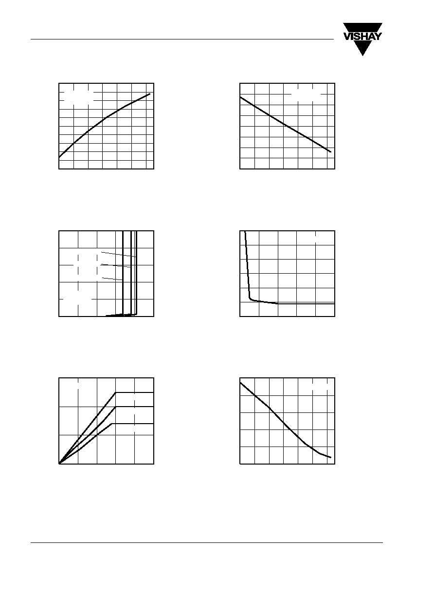
Figure 1. LED Voltage vs. Temperature
Figure 2. LED Forward Current vs. LED Forward Voltage
1.0
1.1
1.2
1.3
1.4
1.5
1.6
≠40
≠20
0
20
40
60
80
Temperature ( C )
17300
I
F
= 50 mA
LED Forward V
oltage ( V )
I
F
= 10 mA
I
F
= 20 mA
I
F
= 5 mA
I
F
= 1 mA
I
F
= 2 mA
0
20
40
60
80
100
120
0.0
0.5
1.0
1.5
2.0
LED Forward Voltage ( V )
17301
T = 85 C
LED Forward Current ( mA
)
T = 25 C
T = ≠40 C
Figure 3. ON-Resistance vs. Temperature
Figure 4. LED Reverse Current vs. LED Reverse Voltage
≠40
≠30
≠20
≠10
0
10
20
30
40
50
60
≠40
≠20
0
20
40
60
80
Ambient Temperature ( C )
17302
I
L
= 50 mA
Normalized to 25 C
Change in On≠Resistance (%)
0
1
2
3
4
5
6
7
8
9
10
0
10
20
30
40
50
60
70
80
LED Reverse Voltage ( V )
17303
T = 85 C
LED Reverse Current (
A
)
T = 25 C
T = ≠40 C
www.vishay.com
4
Document Number 83816
Rev. 1.3, 26-Oct-04
LH1518AAB/ AABTR/ AT
Vishay Semiconductors
Figure 5. Switch Breakdown Voltage vs. Temperature
Figure 6. Switch Breakdown Voltage vs. Load Current
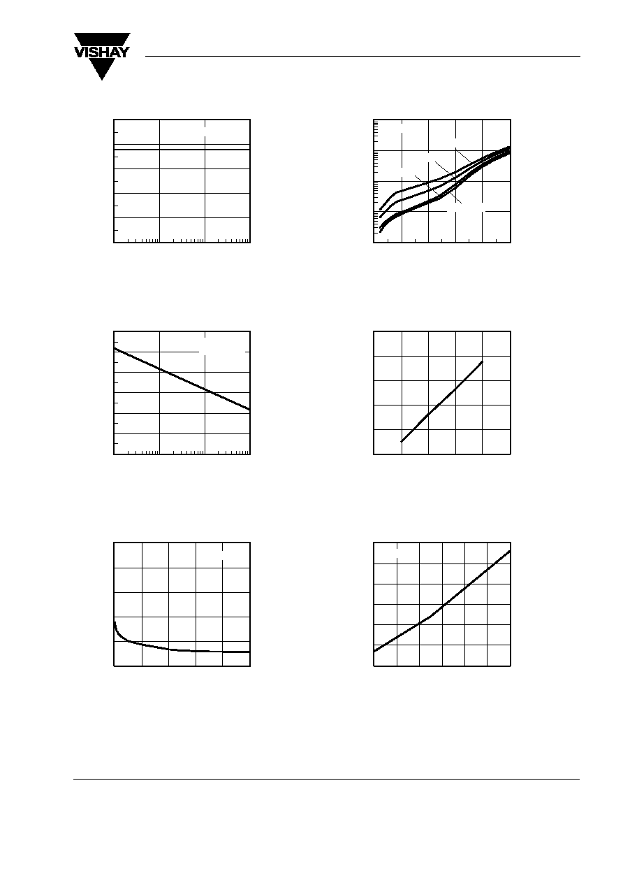
Figure 7. Load Current vs. Load Voltage
≠12
≠10
≠8
≠6
≠4
≠2
0
2
4
6
8
≠40
≠20
0
20
40
60
80
Ambient Temperature ( C )
17304
I
F
= 0
I
L
t50 A
Normalized to 25 C
Change in Breakdown V
oltage ( % )
0
10
20
30
40
50
0
100
200
300
400
500
Load Voltage ( V )
17305
T = 85 C
Load Current (
A
)
T = 25 C
T = ≠40 C
I
F
= 0
I
L
t50 A
0
100
200
300
0
1
2
3
4
5
Load Voltage ( V )
17306
T = 85 C
Load Current ( mA
)
T = 25 C
T = ≠40 C
I
F
= 5 mA
Figure 8. Current Limit vs. Temperature
Figure 9. Variation in ON-Resistance vs. LED Current
Figure 10. LED Dropout Voltage vs. Temperature
≠40
≠30
≠20
≠10
0
10
20
30
40
≠40
≠20
0
20
40
60
80
Ambient Temperature ( C )
17307
I
F
= 5 mA
V
L
= 6 V
Normalized to 25 C
Change in Current Linit ( % )
≠2
0
2
4
6
8
10
0
4
8
12
16
20
LED Current ( mA )
17308
I
L
= 50 mA
norm. at I = 5 mA
F
ac/dc R≠on V
ariation ( % )
1.04
1.08
1.12
1.16
1.20
1.24
≠40
≠20
0
20
40
60
80
Temperature ( C )
17309
I
L
= 100 mA
LED Dropout V
oltage ( V )
LH1518AAB/ AABTR/ AT
Document Number 83816
Rev. 1.3, 26-Oct-04
Vishay Semiconductors
www.vishay.com
5
Figure 11. Insertion Loss vs. Frequency
Figure 12. Output Isolation
Figure 13. Switch Capacitance vs. Applied Voltage
0.00
0.05
0.10
0.15
0.20
0.25
Frequency ( Hz )
17310
R
L
= 600
Insertion Loss ( dB )
100
1000
10000
100000
0
20
40
60
80
100
120
Frequency ( Hz )
17311
R
L
= 50
V
P
= 10 V
Isolation ( dB )
1000
10000
100000
1000000
0
20
40
60
80
100
0
20
40
60
80
100
Applied Voltage ( V )
17312
I
F
= 0
Capacitance ( pF )
Figure 14. Leakage Current vs. Applied Voltage
Figure 15. Switch Offset Voltage vs. LED Current
Figure 16. Switch Offset Voltage vs. Temperature
0
50
100
150
200
250
Load Voltage ( V )
17313
I
F
= 0
Leakage Current ( nA
)
T = 85 C
T = 25 C
T = 70 C
T = 50 C
1
10
100
1000
0.1
0.3
0.4
0.5
0.6
0.7
0.8
0
5
10
15
20
25
LED Current ( mA )
17314
Switch Of
fset V
oltage ( V )
0.0
0.5
1.0
1.5
2.0
2.5
3.0
25
35
45
55
65
75
85
Temperature ( C )
17315
Switch Of
fset V
oltage ( V )
I
F
= 5 mA

www.vishay.com
6
Document Number 83816
Rev. 1.3, 26-Oct-04
LH1518AAB/ AABTR/ AT
Vishay Semiconductors
Figure 17. LED Current for Switch Turn-on vs. Temperature
Figure 18. Turn-off Time vs. LED Current
Figure 19. Turn-on Time vs. LED Current
≠60
≠40
≠20
0
20
40
60
80
100
≠40
≠20
0
20
40
60
80
Temperature ( C )
17316
I
L
= 100 mA
Normalized to 25 C
LED Current for Switch
T
urn≠On ( % )
0.2
0.3
0.4
0.5
0.6
0.7
0.8
0.9
1.0
0
10
20
30
40
50
LED Forward Current ( mA )
17317
T = 85 C
T
urn≠Of
f T
ime
( ms )
T = 25 C
T = ≠40 C
I
L
= 50 mA
0.0
0.5
1.0
1.5
2.0
2.5
3.0
3.5
4.0
0
10
20
30
40
50
LED Forward Current ( mA )
17318
T = 85 C
T
urn≠On
T
ime ( ms )
T = 25 C
T = ≠40 C
I
L
= 50 mA
Figure 20. Turn-off Time vs. Temperature
Figure 21. Turn-on Time vs. Temperature
≠40
≠30
≠20
≠10
0
10
20
30
40
≠40
≠20
0
20
40
60
80
Temperature ( C )
17319
I
F
= 5 mA
I
L
= 50 mA
Normalized to 25 C
Change in
T
urn≠Of
f
T
ime ( % )
≠40
≠20
0
20
40
60
80
100
≠40
≠20
0
20
40
60
80
Temperature ( C )
17320
I
F
= 5 mA
I
L
= 50 mA
Normalized to 25 C
Change in
T
urn≠On
T
ime ( % )

LH1518AAB/ AABTR/ AT
Document Number 83816
Rev. 1.3, 26-Oct-04
Vishay Semiconductors
www.vishay.com
7
Package Dimensions in Inches (mm)
Package Dimensions in Inches (mm)
.014 (.35)
.010 (.25)
.150 (3.81)
.110 (2.79)
.150 (3.81)
.130 (3.30)
.020 (.051) Min.
.300 (7.62)
Typ.
.035 (0.90)
.031 (0.80)
.100 (2.54) Typ.
.039
(1.00)
Min.
.022 (0.55)
.018 (0.45)
.256 (6.50)
.248 (6.30)
.343 (8.70)
.335 (8.50)
Pin One ID.
6
5
4
1
2
3
18
∞ Typ.
.347 (8.82)
.300 (7.62)
4
∞ Typ.
DIP
ISO Method A
i178001
.343 (8.71)
.335 (8.51)
.256 (6.50)
.248 (6.30)
Pin one I.D.
.039
(0.99)
min.
.150 (3.81)
.130 (3.30)
.100 (2.54)
.052 (1.33)
.048 (1.22)
4
∞
.040 (1.016)
.020 (0.508)
.0098 (.25)
.0040 (.10)
.012 (0.31)
.008 (0.20)
.300 (7.62)
.395 (10.03)
.375 (9.63)
3
∞ to 7∞
18
∞
min.
.315 (8.00)
typ.
.050 (1.27) typ.
SMD
ISO Method A
i178002
.100 (2.54)
R .010 (.25)
.070 (1.78)
.030 (.76)
.060 (1.52)
.315 (8.00) min
.435 (11.05)

www.vishay.com
8
Document Number 83816
Rev. 1.3, 26-Oct-04
LH1518AAB/ AABTR/ AT
Vishay Semiconductors
Ozone Depleting Substances Policy Statement
It is the policy of Vishay Semiconductor GmbH to
1. Meet all present and future national and international statutory requirements.
2. Regularly and continuously improve the performance of our products, processes, distribution and
operatingsystems with respect to their impact on the health and safety of our employees and the public, as
well as their impact on the environment.
It is particular concern to control or eliminate releases of those substances into the atmosphere which are
known as ozone depleting substances (ODSs).
The Montreal Protocol (1987) and its London Amendments (1990) intend to severely restrict the use of ODSs
and forbid their use within the next ten years. Various national and international initiatives are pressing for an
earlier ban on these substances.
Vishay Semiconductor GmbH has been able to use its policy of continuous improvements to eliminate the use
of ODSs listed in the following documents.
1. Annex A, B and list of transitional substances of the Montreal Protocol and the London Amendments
respectively
2. Class I and II ozone depleting substances in the Clean Air Act Amendments of 1990 by the Environmental
Protection Agency (EPA) in the USA
3. Council Decision 88/540/EEC and 91/690/EEC Annex A, B and C (transitional substances) respectively.
Vishay Semiconductor GmbH can certify that our semiconductors are not manufactured with ozone depleting
substances and do not contain such substances.
We reserve the right to make changes to improve technical design
and may do so without further notice.
Parameters can vary in different applications. All operating parameters must be validated for each
customer application by the customer. Should the buyer use Vishay Semiconductors products for any
unintended or unauthorized application, the buyer shall indemnify Vishay Semiconductors against all
claims, costs, damages, and expenses, arising out of, directly or indirectly, any claim of personal
damage, injury or death associated with such unintended or unauthorized use.
Vishay Semiconductor GmbH, P.O.B. 3535, D-74025 Heilbronn, Germany
Telephone: 49 (0)7131 67 2831, Fax number: 49 (0)7131 67 2423