0.157 (3.99)
0.177 (4.50)
0.006 (0.152)
0.012 (0.305)
0.030 (0.76)
0.060 (1.52)
0.008 (0.203) MAX.
0.194 (4.93)
0.208 (5.28)
0.100 (2.54)
0.110 (2.79)
0.078 (1.98)
0.090 (2.29)
0.049 (1.25)
0.065 (1.65)
Cathode Band
Mounting Pad Layout
Maximum Ratings and Thermal Characteristics
(T
A
= 25∞C unless otherwise noted)
Parameter
Symbol
B230LA
B240A
Unit
Device marking code
B23
B24
V
Maximum repetitive peak reverse voltage
V
RRM
30
40
V
Maximum RMS voltage
V
RMS
21
28
V
Maximum DC blocking voltage
V
DC
30
40
V
Maximum average forward rectified current
at T
L (See Fig. 1)
I
F(AV)
2.0
A
Peak forward surge current 8.3ms single half
sine-wave superimposed on rated load (JEDEC Method)
I
FSM
50
A
Typical thermal resistance
(2)
R
JA
110
R
JL
28
∞C/W
Voltage rate of change (rated V
R
)
dv/dt
10,000
V/µs
Operating junction temperature range
T
J
-65 to + 150
∞C
Storage temperature range
T
STG
-65 to + 150
∞C
Electrical Characteristics
(T
A
= 25∞C unless otherwise noted)
Parameter
Symbol
Max.
Max.
Unit
Maximum instantaneous
T
J
=25∞C
V
F
0.50
0.55
V
forward voltage at 2.0A
(1)
Maximum DC reverse current
T
J
=25∞C
0.5
0.5
at rated DC blocking voltage
(1)
I
R
mA
Notes: (1) Pulse test: 300
µs pulse width, 1% duty cycle
(2) Aluminum substrate mounted
Features
∑ Low power loss, high efficiency
∑ Low profile surface mount package
∑ Built-in strain relief
∑ For use in low voltage high frequency inverters, free
wheeling, and polarity protection applications
∑ Guardring for overvoltage protection
∑ Plastic package has Underwriters Laboratory
Flammability Classification 94V-0
Mechanical Data
Case: JEDEC DO-214AC molded plastic body
Terminals: Solder plated, solderable per
MIL-STD750, Method 2026
High temperature soldering guaranteed:
250∞C/10 seconds at terminals
Polarity: Color band denotes cathode end
Weight: 0.002 ounce, 0.064 gram
Dimensions in inches
and (millimeters)
DO-214AC (SMA)
0.094 MAX.
(2.38 MAX.)
0.220
(5.58) REF
0.066 MIN.
(1.68 MIN.)
0.052 MIN.
(1.32 MIN.)
B230LA & B240A
Vishay Semiconductors
formerly General Semiconductor
Document Number 88894
www.vishay.com
15-Dec-03
1
New Product
High-Current Density Surface Mount Schottky Rectifier
Reverse Voltage 30 & 40 V
Forward Current 2.0 A
B230LA & B240A
Vishay Semiconductors
formerly General Semiconductor
www.vishay.com
Document Number 88894
2
15-Dec-03
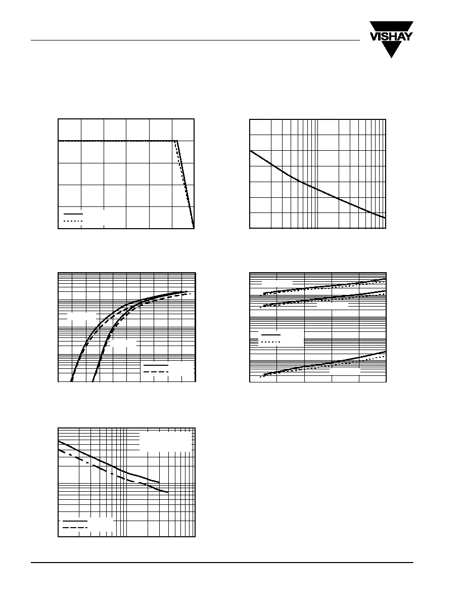
Ratings and
Characteristic Curves
(T
A
= 25∞C unless otherwise noted)
Fig. 5 - Typical Junction Capacitance
C
J
≠ J
unction Capacitance (pF)
100
1,000
10
100
10
1
Reverse Voltage (V)
I
F
≠ Instantaneous F
o
rw
ard Current (A)
Instantaneous Forward Voltage (V)
Fig. 3 - Typical Instantaneous
Forward Characteristics
I
R
≠ Instantaneous Re
v
e
rse Current (mA)
Fig. 4 - Typical Reverse Characteristics
T
J
= 150
∞C
T
J
= 25
∞C
20
0
0.001
0.01
0.1
1.0
10
100
100
40
60
80
Percent of Rated Peak Reverse Voltage (%)
0
1.0
1.5
2.0
2.5
0
25
50
75
100
125
150
Fig. 1 ≠ Forward Current
Derating Curve
A
v
er
age F
o
rw
ard Current (A)
Lead Temperature (
∞C)
0.5
T
J
= 125
∞C
P
eak F
o
rw
ard Surge Current (A)
Number of Cycles at 60 H
Z
Fig. 2 - Maximum Non-Repetitive Peak
Forward Surge Current
0
10
20
30
40
50
60
70
1
10
100
0.01
0.1
0.2
0.4
0.6
0.8
1.0
0.0
1
10
100
T
J
= 25
∞C
T
J
= 125
∞C
0.1
0.3
0.5
0.7
0.9
B230LA
B240A
T
J
= 25
∞C
f = 1.0 MHz
V
sig
= 50 mVp-p
B230LA
B240A
B230LA
B240A
B230LA
B240A