LH1262CAC/ CACTR/ CB
Document Number 83802
Rev. 1.3, 26-Oct-04
Vishay Semiconductors
www.vishay.com
1
i179020
8
7
6
5
1
2
3
4
≠ Output 1
+ Output 1
≠ Output 2
+ Output 2
+ Control 1
≠ Control 1
+ Control 2
≠ Control 2
DIP
SMD
Pb
Pb-free
e3
Dual Photovoltaic MOSFET Driver Solid State Relay
Features
∑ High Open Circuit Voltage
∑ High Short Circuit Current
∑ Isolation Test Voltage 5300 V
RMS
∑ Logic Compatible Input
∑ High Reliability
∑ Lead-free component
∑ Component in accordance to RoHS 2002/95/EC
and WEEE 2002/96/EC
Agency Approvals
∑ UL1577, File No. E52744 System Code H or J,
Double Protection
∑ BSI/BABT Cert. No. 7980
∑ DIN EN 60747-5-2 (VDE0884)
DIN EN 60747-5-5 pending
∑ FIMKO Approval
Applications
High-side Driver
Solid State Relays
Floating Power Supply
Power Control
Data Acquisition
ATE
Isolated Switching
See "Solid Statae Relays" (Application Note 56)
Description
The LH1262CB/CAC Photovoltaic MOSFET Driver
consists of two LEDs optically coupled to two photo-
diode arrays. The photodiode array provides a float-
ing source with adequate voltage and current to drive
high-power MOSFET transistors. Optical coupling
provides a high I/ O Isolation voltage. In order to turn
the MOSFET off, an external resistance (gate-to-
source) is required for gate discharge.
Order Information
Part
Remarks
LH1262CAC
Tubes, SMD-8
LH1262CACTR
Tape and Reel, SMD-8
LH1262CB
Tubes, DIP-8
www.vishay.com
2
Document Number 83802
Rev. 1.3, 26-Oct-04
LH1262CAC/ CACTR/ CB
Vishay Semiconductors
Absolute Maximum Ratings, T
amb
= 25 ∞C
Stresses in excess of the absolute Maximum Ratings can cause permanent damage to the device. Functional operation of the device is
not implied at these or any other conditions in excess of those given in the operational sections of this document. Exposure to absolute
Maximum Ratings for extended periods of time can adversely affect reliability.
SSR
Electrical Characteristics, T
amb
= 25 ∞C
Minimum and maximum values are testing requirements. Typical values are characteristics of the device and are the result of engineering
evaluations. Typical values are for information only and are not part of the testing requirements.
1)
f = 1.0 kHz, pulse width = 100
µs, load (R
L
) = 1.0 M
, 15 pF; measured at 90 % rated voltage (t
on
), 10 % rated voltage (t
off
). Actuation
speed depends upon the external t
on
and t
off
circuitry and the capacitance of the MOSFET.
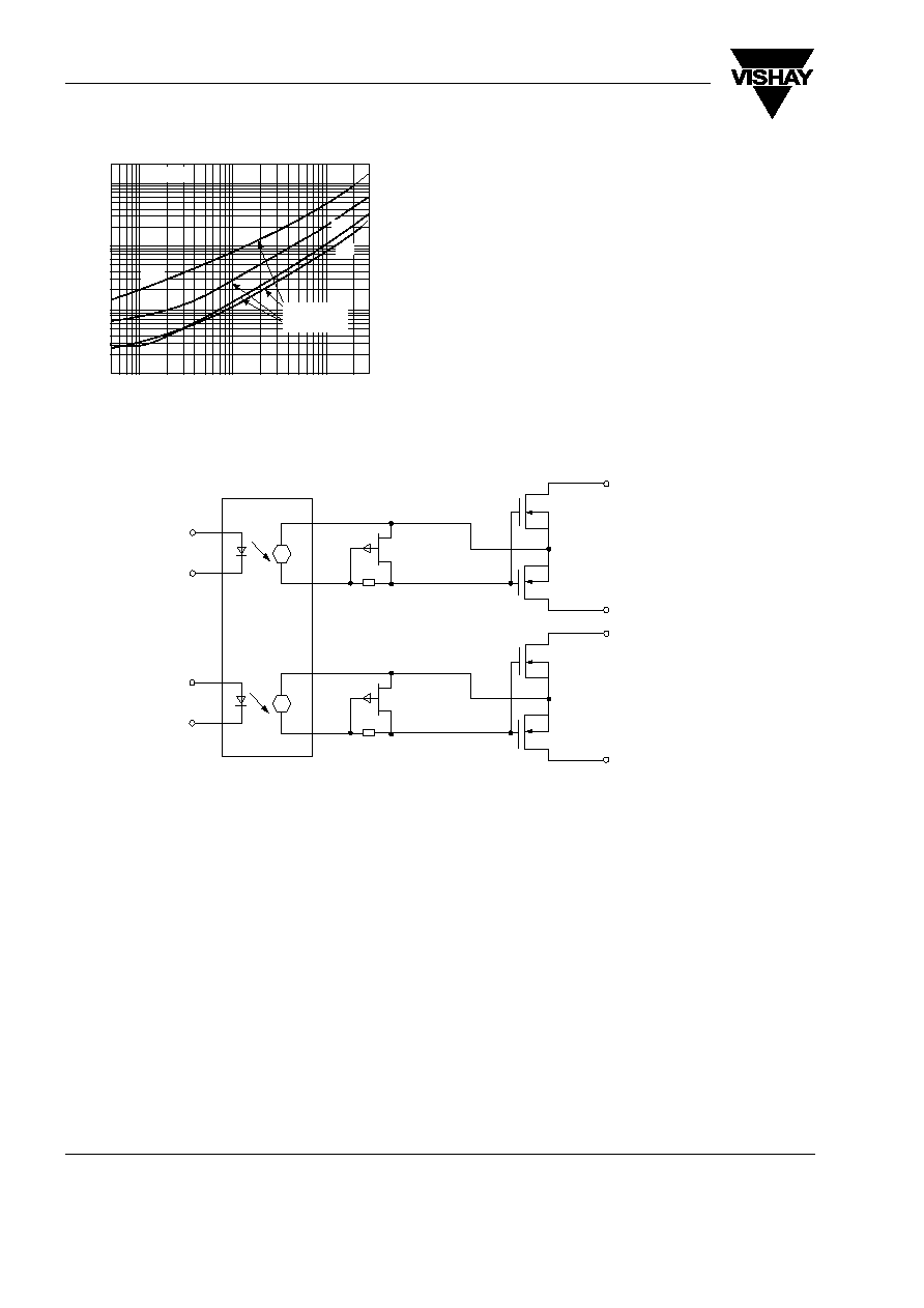
Functional Description
Figure 1 outlines the IV characteristics of the illumi-
nated photodiode array (PDA). For operation at volt-
ages below V
OC
, the PDA acts as a nearly constant
current source. The actual region of operation
depends upon the load.
The amount of current applied to the LED (pins 1 and
2 or 3 and 4) determines the amount of light produced
for the PDA. For high temperature operation, more
LED current may be required.
Parameter
Test condition
Symbol
Value
Unit
LED input ratings continuous forward
current
I
F
50
mA
LED input ratings reverse voltage
I
R
10 µA
V
R
5.0
V
Photodiode array reverse voltage
I
R
2.0 µA
V
R
100
V
Ambient operating temperature range
T
amb
- 40 to + 100
∞C
Storage temperature range
T
stg
- 40 to + 150
∞C
Pin soldering time
t = 7.0 s max.
T
S
270
∞C
Input/output isolation voltage
t = 60 s min.
V
ISO
5300
V
RMS
Parameter
Test condition
Symbol
Min
Typ.
Max
Unit
LED forward voltage
I
F
= 10 mA
V
F
1.15
1.26
1.45
V
Detector forward voltage
I
F
= 10
µA
V
F(PDA)
14
V
Detector reverse voltage
I
R
= 2.0
µA
V
R(PDA)
200
V
Open circuit voltage (pins 5, 6 or 7, 8)
I
F
= 5.0 mA
V
OC
10
12
15
V
I
F
= 10 mA
V
OC
13.1
V
I
F
= 20 mA
V
OC
13.3
V
Short circuit current (pins 5, 6 or 7, 8)
I
F
= 5.0 mA
I
SC
1.0
2.44
6.5
µA
I
F
= 10 mA
I
SC
2.6
5.24
14
µA
I
F
= 20 mA
I
SC
10.8
µA
Turn-on time
I
F
= 20 mA
1)
t
on
35
µs
Turn-off time
I
F
= 20 mA
1)
t
off
90
µs

LH1262CAC/ CACTR/ CB
Document Number 83802
Rev. 1.3, 26-Oct-04
Vishay Semiconductors
www.vishay.com
3
Typical Characteristics (Tamb = 25
∞C unless otherwise specified)
Figure 1. Typical PDA ON Characteristics
Figure 2. Typical PDA ON Characteristics
Figure 3. Typical PDA ON Characteristics
ilh1262cb_01
Open Circuit Voltage (VOC)
Short
Circuit
Current
(I
sc
)
IF=20 mA
IF=5.0 mA
IF=10 mA
10 13.5 14 14.5 +V
17
µA
8
µA
µA
4
ilh1262cb_02
LED Forward Current (mA)
Output
Voltage
(V)
0
4
8
12
16
20
16
14
12
10
8
6
4
2
0
RL=
RL=10 M
RL=5.1 M
RL=2.2 M
RL=1.0 M
ilh1262cb_03
LED Forward Current (mA)
Short
Circuit
Current
(
µ
A)
0
4
8
12
16
20
20
16
12
8
4
0
Figure 4. Typical PDA ON Characteristics
Figure 5. Typical PDA ON Characteristics
Figure 6. Typical PDA ON Characteristics
ilh1262cb_04
Ambient Temperature (∞C)
17
16
15
14
13
12
11
10
0
-40
-20
0
20
40
60
80
100
Open-circuit
Voltage
(V)
IF=20 mA
IF=10 mA
IF=5.0 mA
ilh1262cb_05
Ambient Temperature (∞C)
-40
-20
0
20
40
60
80
100
Short-cirucuit
Current
(
µ
A)
25
20
15
10
5
0
IF=20 mA
IF=10 mA
IF=5.0 mA
ilh1262cb_06
Ambient Temperature (∞C)
LED
Forward
Voltage
(V)
-40
-20
0
20
40
1.6
1.5
1.4
1.3
1.2
1.1
1.0
IF=50 mA
60
80
IF=10 mA
IF=2.0 mA
IF=5.0 mA
IF=20 mA