VISHAY
LH1511BAB/ BABTR/ BT
Document Number 83811
Rev. 1.2, 15-Mar-04
Vishay Semiconductors
www.vishay.com
1
i179031
4
6
5
1
2
3
S'
S
DC
S'
S'
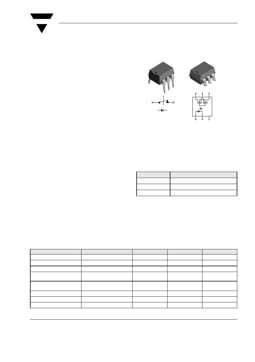
DIP
SMD
1 Form B Solid State Relay
Features
∑ Isolation Test Voltage 3750 V
RMS
∑ Typical R
ON
10
∑ Load Voltage 200 V
∑ Linear, AC/DC Operation
∑ Clean Bounce Free Switching
∑ Low Power Consumption
∑ SMD Lead Available on Tape and Reel
Agency Approvals
∑ UL - File No. E52744
∑ CSA - Certification 093751
∑ BSI
Applications
General Telecom Switching
Security Equipment
Instrumentation
Industrial Controls
Description
The LH1511 relays are SPST normally closed
switches (1 Form B) that can replace electromechan-
ical relays in many applications. The relays are con-
structed as a multi-chip hybrid device. Actuation
control is via an Infrared LED. The output switch is a
combination of a photodiode array with MOSFET
switches and control circuity. The relays can be con-
figured for AC/DC or DC only operation.
Order Information
Absolute Maximum Ratings, T
amb
= 25 ∞C
Stresses in excess of the absolute Maximum Ratings can cause permanent damage to the device. Functional operation of the device is
not implied at these or any other conditions in excess of those given in the operational sections of this document. Exposure to absolute
Maximum Ratings for extended periods of time can adversely affect reliability.
SSR
Part
Remarks
LH1511BAB
Gullwing, Tubes, SMD-6
LH1511BABTR
Gullwing, Tape and Reel, SMD-6
LH1511BT
Tubes, DIP-6
Parameter
Test condition
Symbol
Value
Unit
LED continuous forward current
I
F
50
mA
LED reverse voltage
I
R
10 µA
V
R
8.0
V
DC or peak AC load voltage
I
L
50 µA
V
L
200
V
Continuous DC load current -
bidirectional operation
I
L
200
mA
Continuous DC load current -
unidirectional operation
I
L
300
mA
Peak load current (single shot)
t = 100 ms
I
P
400
mA
Ambient temperature range
T
amb
- 40 to + 85
∞C
Storage temperature range
T
stg
- 40 to + 125
∞C

www.vishay.com
2
Document Number 83811
Rev. 1.2, 15-Mar-04
VISHAY
LH1511BAB/ BABTR/ BT
Vishay Semiconductors
Electrical Characteristics, T
amb
= 25 ∞C
Minimum and maximum values are testing requirements. Typical values are characteristics of the device and are the result of engineering
evaluations. Typical values are for information only and are not part of the testing requirements.
Input
Output
Transfer
Typical Characteristics
(T
amb
= 25
∞C unless otherwise specified)
Pin soldering temperature
t = 10 s max
T
sld
260
∞C
Input/output isolation voltage
V
RMS
t = 1.0 s, I
ISO
= 10
µA max
V
ISO
3750
V
RMS
Output power dissipation
(continuous)
P
diss
550
mW
Parameter
Test condition
Symbol
Min
Typ.
Max
Unit
LED forward current, switch
turn-on
I
L
= ± 200 mA, t = 10 ms
I
Fon
0.2
0.9
mA
LED forward current, switch
turn-off
V
L
= ± 150 V
I
Foff
1.0
2.0
mA
LED forward voltage
I
F
= 10 mA
V
F
1.15
1.26
1.45
V
Parameter
Test condition
Symbol
Min
Typ.
Max
Unit
ON-resistance ac/dc :
Pin 4, 6 (+) to 5 (-)
I
F
= 0 mA, I
L
= 50 mA
R
ON
10
15
ON-resistance dc:
Pin 4, 6 (+) to 5 (-)
I
F
= 0 mA, I
L
= 100 mA
R
ON
2.5
3.75
Off-resistance
I
F
= 5.0 mA, V
L
= ± 100 V
R
OFF
0.1
1.4
G
Off-state leakage current
I
F
= 5.0 mA, V
L
= ± 200 V
0.07
1.0
nA
Output capacitance
I
F
= 5.0 mA, V
L
= 50 V
50
pf
Parameter
Test condition
Symbol
Min
Typ.
Max
Unit
Capacitance (input-output)
V
ISO
= 1.0 V
C
IO
3.0
pF
Turn-on time
I
F
= 10 mA, I
L
= 50 mA
t
on
1.2
3.0
ms
Turn-off time
I
F
= 10 mA, I
L
= 50 mA
t
off
1.0
3.0
ms
Parameter
Test condition
Symbol
Value
Unit
ilh1511bt_00
90
0
60
120
150
30
LOAD
CURRENT
(
mA)
-40
-20
0
20
40
60
80
AMBIENT TEMPERATURE (∞C)
5.0 mA
Fig. 1 Recommended Operating Conditions

www.vishay.com
4
Document Number 83811
Rev. 1.2, 15-Mar-04
VISHAY
LH1511BAB/ BABTR/ BT
Vishay Semiconductors
Ozone Depleting Substances Policy Statement
It is the policy of Vishay Semiconductor GmbH to
1. Meet all present and future national and international statutory requirements.
2. Regularly and continuously improve the performance of our products, processes, distribution and
operatingsystems with respect to their impact on the health and safety of our employees and the public, as
well as their impact on the environment.
It is particular concern to control or eliminate releases of those substances into the atmosphere which are
known as ozone depleting substances (ODSs).
The Montreal Protocol (1987) and its London Amendments (1990) intend to severely restrict the use of ODSs
and forbid their use within the next ten years. Various national and international initiatives are pressing for an
earlier ban on these substances.
Vishay Semiconductor GmbH has been able to use its policy of continuous improvements to eliminate the
use of ODSs listed in the following documents.
1. Annex A, B and list of transitional substances of the Montreal Protocol and the London Amendments
respectively
2. Class I and II ozone depleting substances in the Clean Air Act Amendments of 1990 by the Environmental
Protection Agency (EPA) in the USA
3. Council Decision 88/540/EEC and 91/690/EEC Annex A, B and C (transitional substances) respectively.
Vishay Semiconductor GmbH can certify that our semiconductors are not manufactured with ozone depleting
substances and do not contain such substances.
We reserve the right to make changes to improve technical design
and may do so without further notice.
Parameters can vary in different applications. All operating parameters must be validated for each
customer application by the customer. Should the buyer use Vishay Semiconductors products for any
unintended or unauthorized application, the buyer shall indemnify Vishay Semiconductors against all
claims, costs, damages, and expenses, arising out of, directly or indirectly, any claim of personal
damage, injury or death associated with such unintended or unauthorized use.
Vishay Semiconductor GmbH, P.O.B. 3535, D-74025 Heilbronn, Germany
Telephone: 49 (0)7131 67 2831, Fax number: 49 (0)7131 67 2423
