High Precision Wraparound
Thin Film Chip Resistors
P
Vishay Sfernice
www.vishay.com
For technical questions, contact: sfer@vishay.com
Document Number: 53017
2
Revision: 18-Jul-06
For low noise and precision applications, superior stability,
low temperature coefficient of resistance, and low voltage
coefficient, VISHAY SFERNICE's proven precision thin film
wraparound resistors exceed requirements of
MIL-PRF-55342G characteristics Y (± 10 ppm/∞C).
FEATURES
∑ Load Life Stability at ± 70 ∞C for 2000 hours:
0.1 % under Pn/0.05 % under Pd
∑ Low Temperature Coefficient down to ± 10 ppm/∞C
∑ Very Low Noise < 35 dB a
nd Voltage Coefficient
< 0.01 ppm/V
∑
Resistance Range: 10
to 3 M depending on size
∑
Extended Ohmic Value Range (see table)
∑
Tolerances to ± 0.01 %
∑
In Lot Tracking
5 ppm/∞C
∑
Termination: Thin Film Technology
∑ Gold Plated or Pre-tinned Terminations over Nickel Barrier
∑
Short Circuits (Jumpers) r < 50 mR, I < 2 A
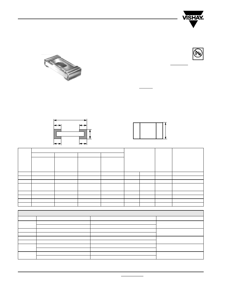
DIMENSIONS in millimeters (inches)
Using special NiCr and CrSi alloys we are able to extend the ohmic value range as indicated above.
* Pb containing terminations are not RoHS compliant, exemptions may apply
Available
Pb-free
RoHS*
COMPLIANT
A
D
D
E
E
C
B
CASE
SIZE
DIMENSION
POWER RATING
mW
LIMITING
ELEMENT
VOLTAGE
RESISTANCE
RANGE (SEE
BELOW FOR
EXTENDED
RANGE)
A
B
C
D/E
MAX. TOL.
MAX. TOL.
MAX. TOL.
MAX. TOL.
+ 0.152 (0.006)
+ 0.127 (0.005)
+ 0.127 (0.005)
+ 0.13 (0.005)
MIN. TOL.
MIN. TOL.
MIN. TOL.
MIN. TOL.
- 0.152 (- 0.006) - 0.127 (- 0.005) - 0.127 (- 0.005)
- 0.13 (- 0.005)
Pn
Pd
V
0402
1.00 (0.040)
0.60 (0.023)
0.5 (0.02)
0.38 (0.015)
50
37
37
10
to 50 k
0505
1.35 (0.053)
1.27 (0.050)
0.5 (0.02)
0.38 (0.015)
125
50
50
10
to 260 k
0603
1.52 (0.060)
0.75 (0.030)
0.5 (0.02)
0.38 (0.015)
125
75
50
10
to 260 k
0705
0805
1.91 (0.075)
1.27 (0.050)
0.5 (0.02)
0.38 (0.015)
200
100
50
10
to 300 k
1005
2.54 (0.100)
1.27 (0.050)
0.5 (0.02)
0.38 (0.015)
250
125
75
10
to 500 k
1206
3.06 (0.120)
1.60 (0.063)
0.5 (0.02)
0.38 (0.015)
330
150
75
10
to 1 M
1505
3.81 (0.150)
1.32 (0.054)
0.5 (0.02)
0.38 (0.015)
350
175
75
10
to 500 k
2010
5.08 (0.200)
2.54 (0.100)
0.5 (0.02)
0.38 (0.015)
1000
500
100
10
to 3 M
EXTENDED OHMIC VALUE RANGE FOR HIGH PRECISION WRAPAROUND THIN FILM CHIP RESISTORS
SIZE
TIGHTEST TOLERANCE %
EXTENDED OHMIC VALUE RANGE
BEST TCR (ppm/∞C)
0402
0.05
50 k - 100 k
25
0.1
100 k - 1 M
50
0505
0.05
250 k - 300 k
25
0603
0.1
300 k - 2 M5
50
0705
0.05
300 k - 500 k
25
0805
0.1
500 k - 5 M
50
1206
0.05
1 M - 2 M
25
0.1
2 M - 15 M
50
2010
0.05
3 M - 6 M
25
0.25
6 M - 50 M
50

P
High Precision Wraparound
Thin Film Chip Resistors
Vishay Sfernice
Document Number: 53017
For technical questions, contact: sfer@vishay.com
www.vishay.com
Revision: 18-Jul-06
3
ELECTRICAL SPECIFICATIONS
Resistance Range:
10
to 3 M
Resistance Tolerance:
± 0.1 % to ± 5 %
± 0.01 % to ± 0.05 % on Y type
Power Dissipation:
Pn: 50 mW to 1 W
Pd: 37 mW to 500 mW
on tolerance tighter than ± 0.05 %
Temperature Coefficient: see table below
MECHANICAL SPECIFICATIONS
Substrate:
Alumina
Technology:
Thin Film
Film:
Nickel Chromium with mineral
passivation or Ta
2
N
Protection:
Silicon
Terminations:
B type: SnPb over nickel barrier
for solder reflow
N type: SnAg over nickel barrier
G type: gold over nickel barrier
for other applications
CLIMATIC SPECIFICATIONS
Operating Temp. Range: - 55 ∞C to + 155 ∞C
For temperature up to 200 ∞C, please consult factory
* R > 50
on request for lower values
POWER DERARING CURVE
PACKAGING
Several types of packaging are available: tube, waffle-pack, and
tape and reel.
* 12 mm on request
* 0.05 % under Pd
TEMPERATURE COEFFICIENT
TCR
CODE
FILM
± 10 ppm/∞C*
Y
Ni Cr
± 25 ppm/∞C
E
Ni Cr
± 50 ppm/∞C
H
Ni Cr or Ta
2
N
± 100 ppm/∞C
K
Ni Cr or Ta
2
N
SIZE
NUMBER OF PIECES PER PACKAGE
TAPE
WIDTH
TUBE
WAFFLE
PACK
2" ◊ 2"
TAPE AND REEL
MIN.
MAX.
0402
500
100
100
4000
8 mm
0505
0603
0805
0705
1005
500
140
1206
1505
60
2010
100
100
2000
8 mm*
BEST TOL. AND TCR V RESISTANCE VALUE
TIGHTEST
TOLERANCE
CODE
OHMIC VALUES
TCR
ppm/∞C
± 0.25 %
C
R > 10
± 25
± 0.10 %
B
R > 25
± 20
± 0.05 %
W
R > 50
± 10
± 0.02 %
P
R > 100
± 0.01 %
L
R > 250
R
E
W
O
P
D
E
T
A
R
%
100
80
60
40
20
0
0 20 40 60 70 80 100 120 140 155
AMBIENT TEMPERATURE IN ∞C
PERFORMANCE
TESTS
CONDITIONS
Ta
2
N
DRIFTS
Ni Cr
MIL-PRF-55342G
Requirements
Typical
Performances
MIL-PRF-55342G
Typical
Performances
Thermal Shock
MIL-PRF-55342G
MIL-STD-202 F-Method 107 F
± 0.25 %
± 0.02 %
± 0.05 %
± 0.02 %
Short Time Overload
MIL-PRF-55342G
Para 3.10.4.7.5
± 010 %
± 0.01 %
± 0.05 %
± 0.01 %
Low Temperature Operation
MIL-PRF-55342G
Para 3.9 & 4.7.4
± 0.25 %
± 0.01 %
± 0.05 %
± 0.01 %
Resistance to Solder Heat
MIL-PRF-55342G
Para 3.12, 4.7.7, 4.7.1.2
± 0.25 %
± 0.04 %
± 0.05 %
± 0.03 %
Moisture Resistance
MIL-PRF-55342G
Para 3.13 & 4.7.8
MIL-STD-202 F-Method 106 E
± 0.40 %
± 0.01 %
± 0.10 %
± 0.01 %
High Temperature
MIL-PRF-55342G
Para 3.11 & 4.7.6
± 0.20 %
± 0.075 %
± 0.05 %
± 0.05 %
Load Life
MIL-PRF-55342G
2000 hours Pn at 70 ∞C
MIL-STD-202 F-Method 108 A
± 0.50 %
± 0.15 %
± 0.5 %
± 0.10 %*
P
Vishay Sfernice
www.vishay.com
For technical questions, contact: sfer@vishay.com
Document Number: 53017
4
Revision: 18-Jul-06
Chips ready to be trimmed available. (P
trim
) - Please consult Sfernice.
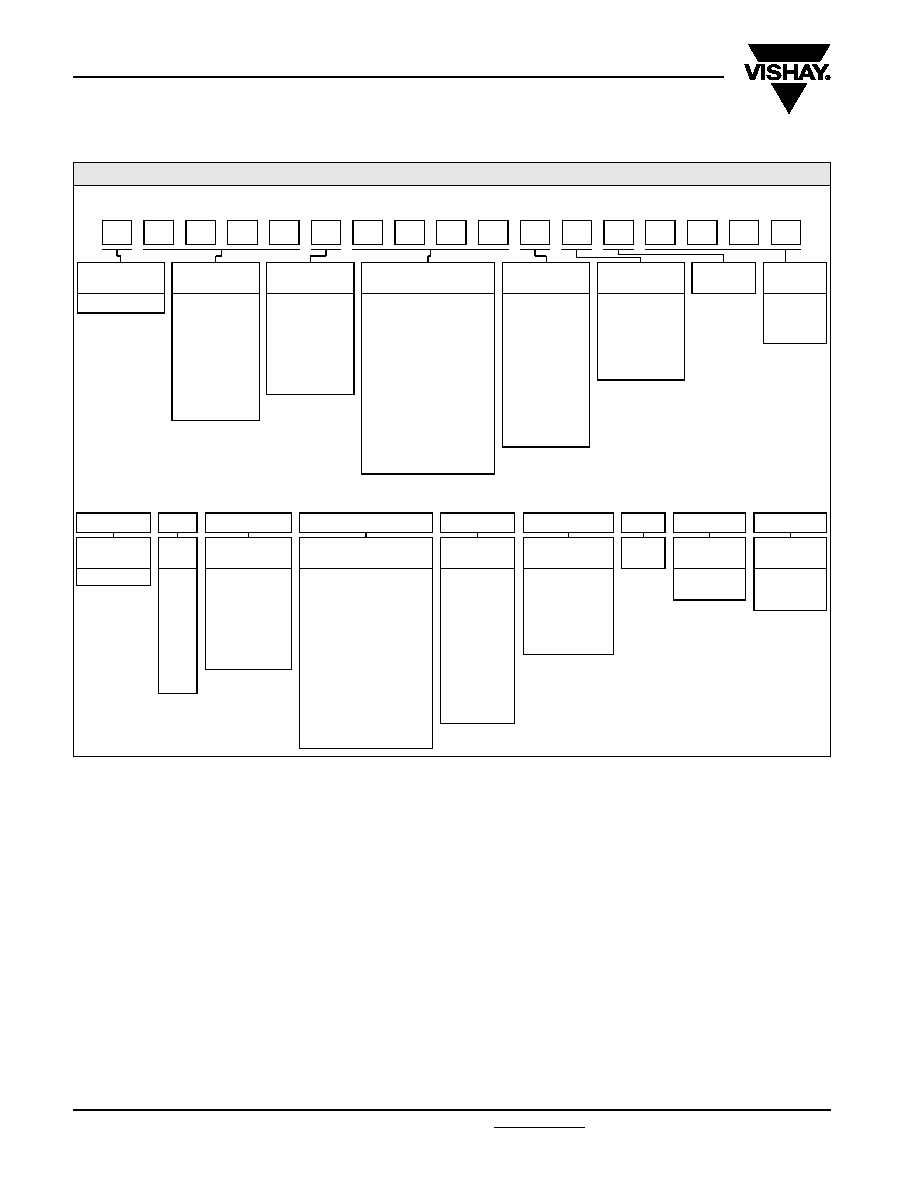
GLOBAL PART NUMBER INFORMATION
New Global Part Numbering: P0505Y1003BBT0933
GLOBAL
MODEL
SIZE
TCR
VALUE
TOLERANCE
TERMINATION
TAPE
OPTION
P
0402
0505
0603
0705
0805
1005
1206
1505
2010
K = ± 100 ppm/∞C
H = ± 50 ppm/∞C
E = ± 25 ppm/∞C
Y = ± 10 ppm/∞C
X = Jumper
Z = ± 5 ppm
(0.70 ∞C)
The first three digits (2
digits are enough for
tolerance G and J) are
significant figures and
the last digit specifies
the number of zeros to
follow, R designates
decimal point
10R0 = 10
3901 = 3900
1004 = 1 M
0R00 = Jumper
L = ± 0.01 %
P = ± 0.02 %
W = ± 0.05 %
B = ± 0.1 %
C = ± 0.25 %
D = ± 0.5 %
F = ± 1 %
G = ± 2 %
J = ± 5 %
S = Special
X = Jumper
B: SnPb over
nickel barrier
N: SnAg over
nickel barrier
G: Gold over
nickel barrier
Leave
blank if no
option
B: Lead bearing version
N and G: Lead
(Pb)-free/RoHS version
Historical Part Number example: P 0505 Y 1003 B B TR R0933 e2
P
0505
Y
1003
B
B
TR
R0933
e2
HISTORICAL
MODEL
SIZE
TCR
VALUE
TOLERANCE
TERMINATION
TAPE
OPTION
RoHS
P
0402
0505
0603
0705
0805
1005
1206
1505
2010
K = ± 100 ppm/∞C
H = ± 50 ppm/∞C
E = ± 25 ppm/∞C
Y = ± 10 ppm/∞C
X = Jumper
Z = ± 5 ppm
(0.70 ∞C)
The first three digits (2
digits are enough for
tolerance G and J) are
significant figures and
the last digit specifies
the number of zeros to
follow, R designates
decimal point
10R0 = 10
3901 = 3900
1004 = 1 M
0R00 = Jumper
L = ± 0.01 %
P = ± 0.02 %
W = ± 0.05 %
B = ± 0.1 %
C = ± 0.25 %
D = ± 0.5 %
F = ± 1 %
G = ± 2 %
J = ± 5 %
S = Special
X = Jumper
B: SnPb over
nickel barrier
N: SnAg over
nickel barrier
G: Gold over
nickel barrier
Leave blank
if no option
e2: tin/silver
e4: gold
blank: SnPb
B: Lead bearing version
N and G: Lead
(Pb)-free/RoHS version
0
5
0
5
Y
1
0
0
3
P
B
B
T
0
9
3
3

Legal Disclaimer Notice
Vishay
Document Number: 91000
www.vishay.com
Revision: 08-Apr-05
1
Notice
Specifications of the products displayed herein are subject to change without notice. Vishay Intertechnology, Inc.,
or anyone on its behalf, assumes no responsibility or liability for any errors or inaccuracies.
Information contained herein is intended to provide a product description only. No license, express or implied, by
estoppel or otherwise, to any intellectual property rights is granted by this document. Except as provided in Vishay's
terms and conditions of sale for such products, Vishay assumes no liability whatsoever, and disclaims any express
or implied warranty, relating to sale and/or use of Vishay products including liability or warranties relating to fitness
for a particular purpose, merchantability, or infringement of any patent, copyright, or other intellectual property right.
The products shown herein are not designed for use in medical, life-saving, or life-sustaining applications.
Customers using or selling these products for use in such applications do so at their own risk and agree to fully
indemnify Vishay for any damages resulting from such improper use or sale.