 | –≠–ª–µ–∫—Ç—Ä–æ–Ω–Ω—ã–π –∫–æ–º–ø–æ–Ω–µ–Ω—Ç: SiP4280A | –°–∫–∞—á–∞—Ç—å:  PDF PDF  ZIP ZIP |
Vishay Siliconix
SiP4280A
Document Number: 73602
S-61772≠Rev. C, 11-Sep-06
www.vishay.com
1
Slew Rate Controlled Load Switch
FEATURES
∑ 1.5 V to 5.5 V Input Voltage range
∑ Very Low R
DS(ON)
, typically 80 m
(5 V)
∑ Slew rate limited turn-on time options
- SiP4280A-1: 1 ms
- SiP4280A-3: 100 µs
∑ Fast shutdown load discharge option
∑ Low quiescent current
< 25 nA (typ)
∑ 4 kV ESD Rating
∑ 6 pin SOT23 package
APPLICATIONS
∑ Cellular telephones
∑ Digital still cameras
∑ Personal digital assistants (PDA)
∑ Hot swap supplies
∑ Notebook computers
∑ Personal communication devices
DESCRIPTION
The SiP4280A is a P-Channel MOSFET power switch
designed for high-side load switching applications. The
output pass transistor is a P-Channel MOSFET tran-
sistor with typically 80 m
R
DS(ON)
. The SiP4280A is
available in two different versions of turn-on times. The
SiP4280A-1 version has a slew rate limited turn-on
time typically of 1 ms. The SiP4280A-3 version has a
slew rate limited turn-on time typically of 100 µs and
additionally offers a shutdown load discharge circuit to
rapidly turn off a load circuit when the switch is dis-
abled.
Both SiP4280A load switch versions operate with an
input voltage ranging from 1.5 V to 5.5 V, making them
ideal for both 3 V and 5 V applications. The SiP4280A
also features an under-voltage lock out which turns the
switch off when an input undervoltage condition exists.
Input logic levels are TTL and 2.5 V to 5.0 V CMOS
compatible. The quiescent supply current is very low,
typically 25 nA. In shutdown mode, the supply current
decreases to less than 1.0 µA.
The SiP4280A is available in a 6 pin SOT23 package
and is specified over - 40 ∞C to 85 ∞C temperature
range.
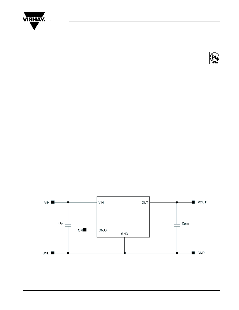
TYPICAL APPLICATION CIRCUIT
SiP4280A
1 µF
0.1 µF
www.vishay.com
2
Document Number: 73602
S-61772≠Rev. C, 11-Sep-06
Vishay Siliconix
SiP4280A
Notes:
a. Device mounted with all leads soldered or welded to PC board.
b. Derate 5.5 mW/∞C above T
A
= 70 ∞C.
Stresses beyond those listed under "Absolute Maximum Ratings" may cause permanent damage to the device. These are stress ratings only,
and functional operation of the device at these or any other conditions beyond those indicated in the operational sections of the specifications is
not implied. Exposure to absolute maximum rating/conditions for extended periods may affect device reliability.
Notes:
a. The algebraic convention whereby the most negative value is a minimum and the most positive a maximum.
b. Typical values are for DESIGN AID ONLY, not guaranteed nor subject to production testing.
d. For V
IN
1.5 V see typical ON/OFF threshold curve.
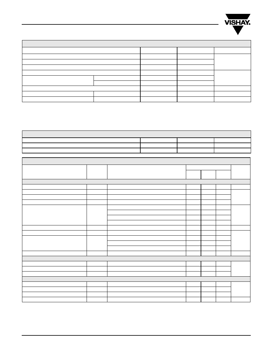
ABSOLUTE MAXIMUM RATINGS
Parameter Symbol
Steady
State
Unit
Supply Input Voltage
V
IN
- 0.3 to 6
V
Enable Input Voltage
V
ON
- 0.3 to 6
Output Voltage
V
OUT
- 0.3 to V
IN
+ 0.3
Maximum Switch Current
I
MAX
2.3
A
Maximum Pulsed Current
V
IN
2.5
I
DM
6
V
IN
< 2.5
I
DM
3
Junction Temperature
T
J
- 40 to 150
∞C
Thermal Resistance
SOT23-6L
JA
a
180
∞C/W
Power Dissipation
SOT23-6L
b
P
D
440
mW
RECOMMENDED OPERATING RANGE all voltages referenced to GND = 0 V
Parameter Symbol
Steady
State
Unit
V
IN
1.5 to 5.5
V
Operating Temperature Range
- 40 to 85
∞C
SPECIFICATIONS
Parameter Symbol
Test Conditions Unless Specified
V
IN
= 5 V, T
A
= - 40 to 85 ∞C
Limits
Min
a
Typ
b
Max
a
Unit
SiP4280A All Versions
Operating Voltage
V
IN
1.5
-
5.5
V
Quiescent Current
I
Q
ON/OFF = active
-
1
µA
Off Supply Current
I
Q(OFF)
ON/OFF = inactive, OUT = open
-
0.01
1
Off Switch Current
I
SD(OFF)
ON/OFF = inactive, V
OUT
= 0
-
0.01
1
On-Resistance
R
DS(ON)
V
IN
= 5 V, T
A
= 25 ∞C
-
80
120
m
V
IN
= 4.2 V, T
A
= 25 ∞C
-
85
130
V
IN
= 3 V, T
A
= 25 ∞C
-
100
150
V
IN
= 1.8 V, T
A
= 25 ∞C
-
160
250
On-Resistance Temp-Coefficient
TC
RDS
-
2800
-
ppm/∞C
ON/OFF Input Low Voltage
c
V
IL
V
IN
= 1.8 V to 5.5 V
-
-
0.4
V
ON/OFF Input High Voltage
V
IH
V
IN
= 1.5 V to 2.7 V
1.4
-
-
V
IN
= 2.7 V to
< 4.2 V
2
-
-
V
IN
4.2 V to 5.5 V
2.4
-
-
ON/OFF Input Leakage
I
SINK
V
ON/OFF
= 5.5 V
-
-
1
µA
SiP4280A-1 Version
Output Turn-On Delay Time
T
D(ON)
V
IN
= 5 V, R
LOAD
= 10
, T
A
= 25 ∞C
-
20
40
µs
Output Turn-On Rise Time
T
ON
V
IN
= 5 V, R
LOAD
= 10
, T
A
= 25 ∞C
-
1000
1500
Output Turn-Off Delay Time
T
D(OFF)
V
IN
= 5 V, R
LOAD
= 10
, T
A
= 25 ∞C
-
4
10
SiP4280A-3 Version
Output Turn-On Delay Time
T
D(ON)
V
IN
= 5 V, R
LOAD
= 10
, T
A
= 25 ∞C
-
20
40
µs
Output Turn-On Rise Time
T
ON
V
IN
= 5 V, R
LOAD
= 10
, T
A
= 25 ∞C
-
100
150
Output Turn-Off Delay Time
T
D(OFF)
V
IN
= 5 V, R
LOAD
= 10
, T
A
= 25 ∞C
-
4
10
Output Pull-Down Resistance
R
PD
ON/OFF = inactive, T
A
= 25 ∞C
-
150
250
Document Number: 73602
S-61772≠Rev. C, 11-Sep-06
www.vishay.com
3
Vishay Siliconix
SiP4280A
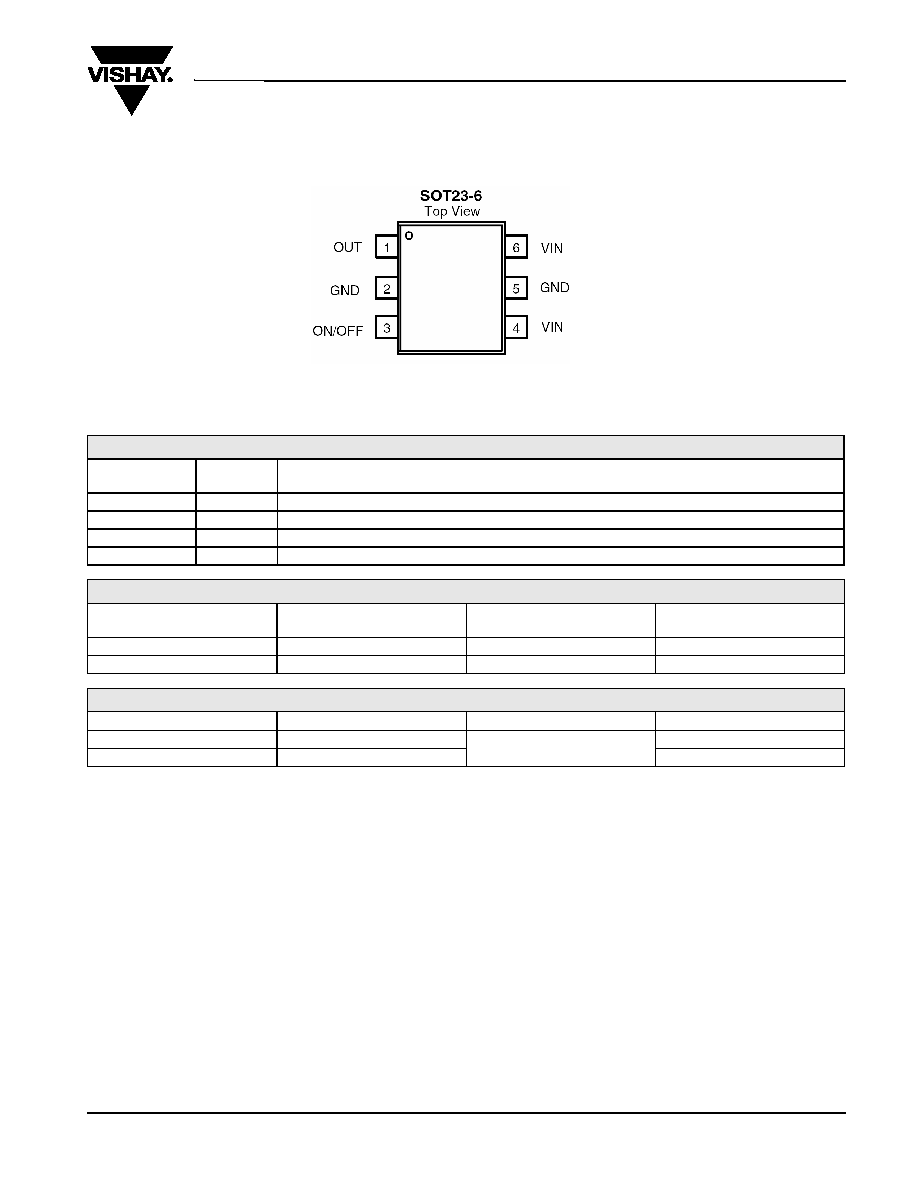
PIN CONFIGURATION
PIN DESCRIPTION
Pin Number
SOT23-6 Pin
Name
Description
4, 6
V
IN
This pin is the P-Channel MOSFET source connection
3
ON/OFF
Logic high enables the IC; logic low disables the IC
2, 5
GND
Ground connection
1
OUT
This pin is the P-Channel MOSFET drain connection
SELECTION GUIDE
Part Number
Slew Rate
(typ)
Active
Pull Down
Enable
SiP4280A-1-T1-E3
1 ms
No
Active High
SiP4280A-3-T1-E3
100 µs
Yes
Active High
ORDERING INFORMATION
Part Number
Marking
Temperature Range
Package
SiP4280ADT-1-T1-E3
L4XX
- 40 ∞C to 85 ∞C
SOT23-6L
SiP4280ADT-3-T1-E3
L6XX
SOT23-6L
www.vishay.com
4
Document Number: 73602
S-61772≠Rev. C, 11-Sep-06
Vishay Siliconix
SiP4280A
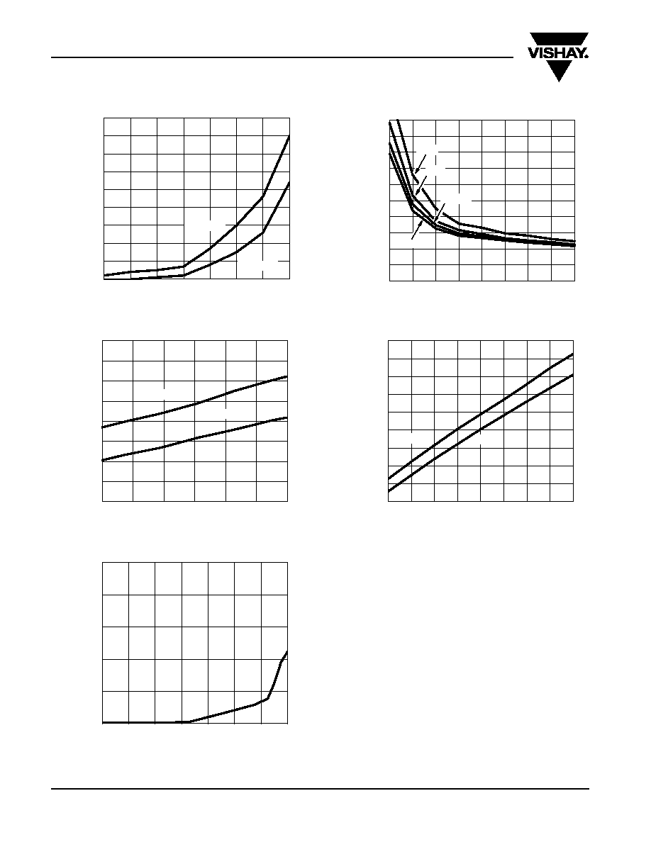
TYPICAL CHARACTERISTICS internally regulated, 25 ∞C unless noted
Quiescent Current vs. Temperature
R
DS(ON)
vs. Temperature
Off Switch Current vs. Temperature
0
10
20
30
40
50
60
70
80
90
- 40
- 20
0
20
40
60
80
100
Temperature (∞C)
V
IN
= 5 V
V
IN
= 3 V
I
Q
)
A
n
(
60
70
80
90
100
110
120
130
140
Temperature (∞C)
r
)
N
O
(
S
D
(m
)
- 40
- 25
0
25
50
75
85
V = 5 V
V = 3 V
0.0
0.2
0.4
0.6
0.8
1.0
- 40
- 20
0
20
40
60
80
100
Temperature (∞C)
(µA)
W
S
f
f
o
I
R
DS(ON)
vs. Input Voltage
ON/OFF Threshold vs. Input Voltage
50
70
90
110
130
150
170
190
210
230
250
1.5
2.0
2.5
3.0
3.5
4.0
4.5
5.0
5.5
V
IN
(V)
2 A
100 mA
1 A
500 mA
r
)
N
O
(
S
D
(m
)
0.4
0.6
0.8
1.0
1.2
1.4
1.6
1.8
2.0
2.2
1.5
2.0
2.5
3.0
3.5
4.0
4.5
5.0
5.5
V
IN
(V)
V
IL
)
V
(
d
l
o
h
s
e
r
h
T
F
F
O
/
N
O
V
IH
Document Number: 73602
S-61772≠Rev. C, 11-Sep-06
www.vishay.com
5
Vishay Siliconix
SiP4280A
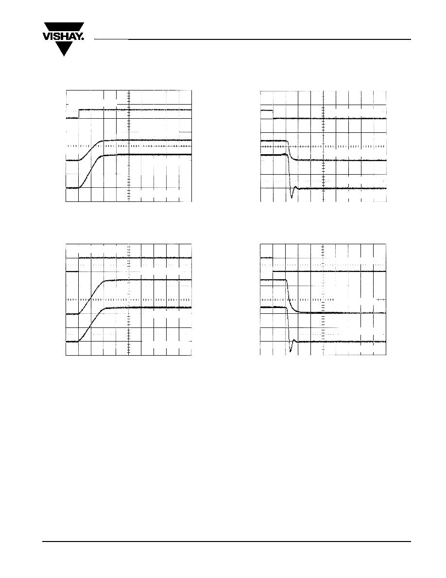
TYPICAL WAVEFORMS
SiP4280A-1 Turn-On (V
IN
= 3 V, R
LOAD
= 6
)
SiP4280A-1 Turn-On (V
IN
= 5 V, R
LOAD
= 10
)
ON/OFF (5 V/div.)
V
OUT
(2 V/div.)
I
IN
(200 mA/div.)
Time (500 µ s/div)
ON/OFF (5 V/div.)
V
OUT
(2 V/div.)
I
IN
(200 mA/div.)
Time (500 µ s/div)
SiP4280A-1 Turn-Off (V
IN
= 3 V, R
LOAD
= 6
)
SiP4280A-1 Turn-Off (V
IN
= 5 V, R
LOAD
= 10
)
ON/OFF (5 V/div.)
V
OUT
(2 V/div.)
I
IN
(200 mA/div.)
Time (5 µs/div)
ON/OFF (5 V/div.)
V
OUT
(2 V/div.)
I
IN
(200 mA/div.)
Time (5 µ s/div)