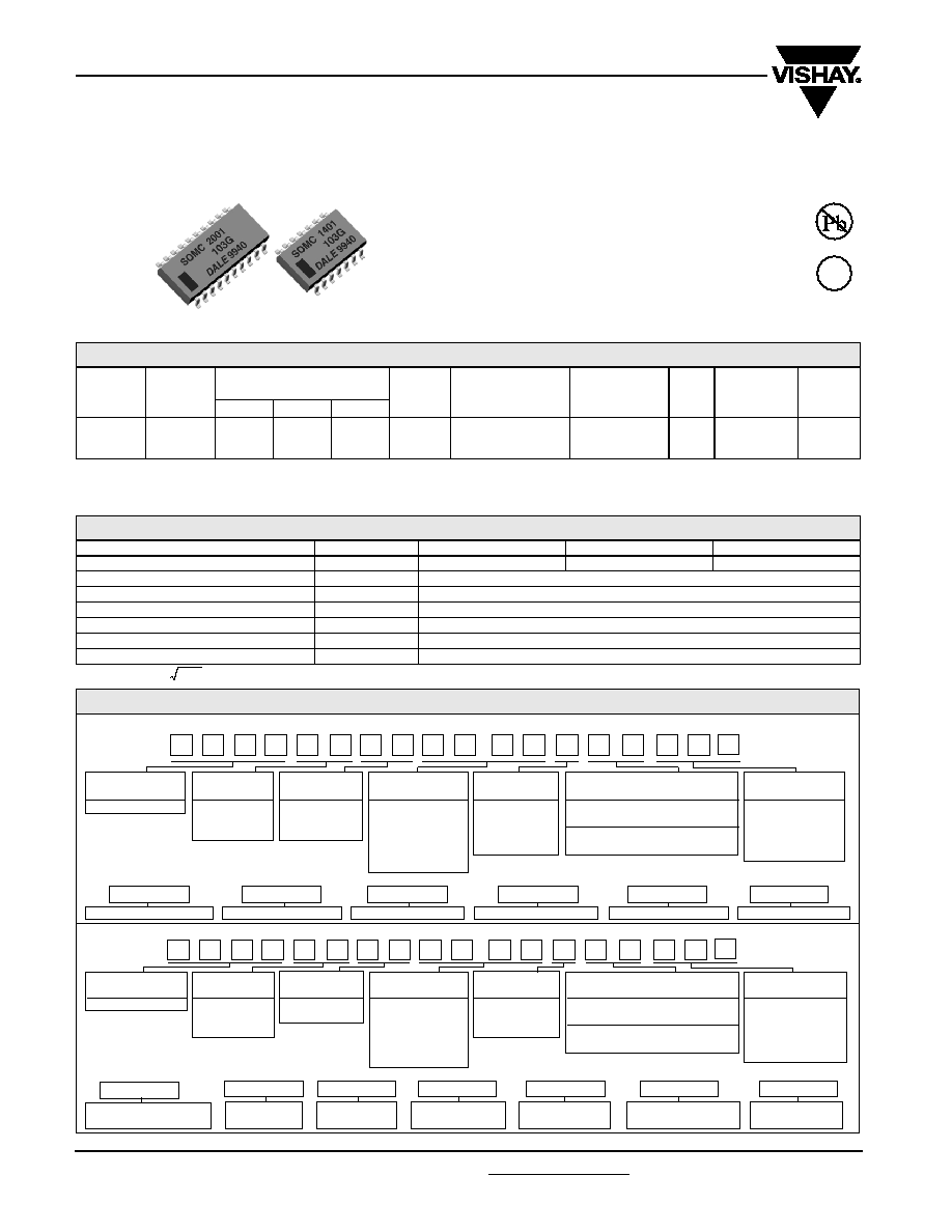
Thick Film, Dual-in-Line Resistor Networks
www.vishay.com
For technical questions, contact: ff2aresistors@vishay.com
Document Number: 31508
38
Revision: 21-Aug-06
SOMC
Vishay Dale
FEATURES
∑
14,16 or 20 terminal package
∑ Isolated, bussed or TTL-terminator circuits
∑ Molded case construction
∑ Thick film resistive elements
∑ Reflow solderable
∑ Compatible with automatic surface mounting equipment
∑ Reduces total assembly costs
∑ For wave flow soldering contact factory
∑ Lead (Pb)-free version is RoHS compliant
1)
Temperature Range: - 55 ∞C to + 125 ∞C
∑ Power rating depends on the max. temperature at the solder point, the component placement density and the substrate material
∑ Jumper: Zero-Ohm-Resistor on request (100 m
)
∑ Packaging: according to EIA; see appropriate catalog or web page
2)
Rated voltage:
* Pb containing terminations are not RoHS compliant, exemptions may apply
Available
RoHS*
COMPLIANT
e1
STANDARD ELECTRICAL SPECIFICATIONS
GLOBAL
MODEL
ELEMENT
P
70 ∞C
W
PACKAGE POWER RATING
P
70 ∞C
W
CIRCUIT
LIMITING
ELEMENT
VOLTAGE MAX.
V
TEMPERATURE
COEFFICIENT
1)
ppm/∞C
TOL.
%
RESISTANCE
RANGE
E-SERIES
14
16
20
SOMC
0.08
0.16
0.08
1.05
1.125
1.05
1.20
1.28
1.20
1.52
1.60
1.52
01
03
05
50
100
1, 2, 5
1, 2, 5
1, 2, 5
10R - 1M
24
TECHNICAL SPECIFICATIONS
PARAMETER
UNIT
01 CIRCUIT
03 CIRCUIT
05 CIRCUIT
Rated Dissipation at 70 ∞C per Element
W
0.08
0.16
0.08
Limiting Element Voltage
2)
V
50
Voltage Coefficient
ppm/V
< 50
Insulation Voltage (1min)
V
dc/ac
peak
200
Category Temperature Range
∞C
- 55/+ 150
Insulation Resistance
> 10
10
TC Tracking (- 55 ∞C to + 125 ∞C)
ppm/∞C
50
PxR
VALUE 1
S
O
M
C
1
6
0
1
1
K
0
0
G
D
C
New Global Part Numbering: SOMC16011K00GDC (preferred part numbering format)
GLOBAL MODEL
PIN COUNT
SCHEMATIC
RESISTANCE
TOLERANCE
PACKAGING
SPECIAL
VALUE CODE
SOMC
14
01 = Bussed
R = Decimal
F = ± 1 %
EJ = Lead Free, Tube
Blank = Standard
16
03 = Isolated
K = Thousand
G = ± 2 %
EA = Lead Free, Tape & Reel
(Dash Number)
20
00 = Special
M = Million
J = ± 5 %
DC = Tin/Lead, Tube
(up to 3 digits)
10R0 = 10
S = Special
RZ = Tin/Lead, Tape & Reel
From 1-999
680K = 680 k
as applicable
1M00 = 1.0 M
GLOBAL PART NUMBER INFORMATION
HISTORICAL MODEL
PIN COUNT
SCHEMATIC
RESISTANCE VALUE
TOLERANCE CODE
PACKAGING
SOMC
16
01
102
G
D02
Historical Part Number example: SOMC1601102G (will continue to be accepted)
SOMC
20
05
810
131
G
R61
S
O
M
C
2
0
0
5
5
0
0
B
G
R
Z
Historical Part Number example: SOMC2005820131G (will continue to be accepted)
New Global Part Numbering: SOMC2005500BGRZ (preferred part numbering format)
GLOBAL MODEL
PIN COUNT
SCHEMATIC
RESISTANCE
TOLERANCE
PACKAGING
SPECIAL
VALUE
CODE
SOMC
14
05 = Dual
3 digit
F = ± 1 %
EJ = Lead Free, Tube
Blank = Standard
16
Terminator
Impedence code,
G = ± 2 %
EA = Lead Free, Tape & Reel
(Dash Number)
20
followed by
J = ± 5 %
DC = Tin/Lead, Tube
(up to 3 digits)
Alpha modifier
RZ = Tin/Lead, Tape & Reel
From 1-999
(see Impedence
as applicable
table
HISTORICAL MODEL
PIN COUNT
SCHEMATIC
RESISTANCE
RESISTANCE
TOLERANCE
PACKAGING
CODE
VALUE 2
Document Number: 31508
For technical questions, contact: ff2aresistors@vishay.com
www.vishay.com
Revision: 21-Aug-06
39
SOMC
Thick Film, Dual-in-Line Resistor Networks
Vishay Dale
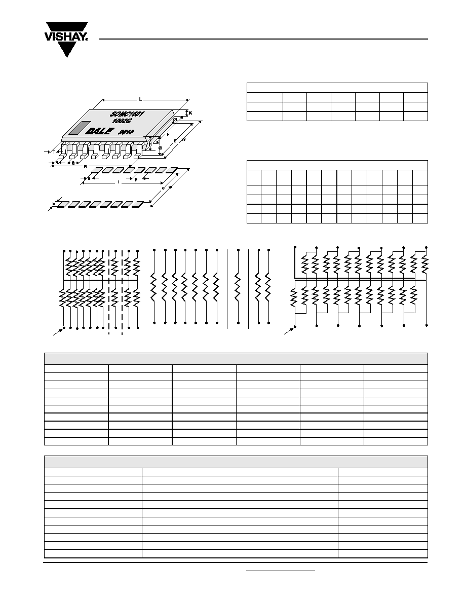
DIMENSIONS
The dimension shown are for a 16 pin part. For parts with different
pin numbers use the same pitch and add or subtract pads as
required.
NOTE: Maximum solder reflow temperature + 255 ∞C
CIRCUIT SCHEMATICS
Pin 1
SOLDER PAD DIMENSIONS in inches [millimeters]
a
b
c
l
p
w
WAVE
0.64
1.91
5.34
9.53
1.27
9.15
REFLOW
0.64
1.91
5.34
9.53
1.27
9.15
DIMENSIONS [in millimeters]
PIN
NO#
L
W
B
E
F
G
H
K
R
S
T
14
9.91
7.62
7.62
6.20
5.59
2.16
2.03
0.914 0.457
1.27
1.14
16
11.18
7.62
8.89
6.20
5.59
2.16
2.03
0.914 0.457
1.27
1.14
20
13.72
7.62
11.43
6.20
5.59
2.16
2.03
0.914 0.457
1.27
1.14
Tol ± 0.254 ± 0.381 ± 0.254 ± 0.381 ± 0.127 ± 0.127 ± 0.127
± 0.254
R1
R1
R1
R1
R1
R1
R1
R1
R1
R1
R1
R1
R2
R2
R2
R2
R2
R2
R2
R2
R2
R2
R2
R2
05 Circuit
14 pin
Pin 1
01 Circuit
14 pin
16
20 pin
pin
Pin 1
03 Circuit
14 pin
16 pin 20 pin
IMPEDANCE CODES
CODE
R
1
(
)
R
2
(
)
CODE
R
1
(
)
R
2
(
)
500B
82
130
141A
270
270
750B
120
200
181A
330
390
800C
130
210
191A
330
470
990A
160
260
221B
330
680
101C
180
240
281B
560
560
111C
180
270
381B
560
1.2K
121B
180
390
501C
620
2.7K
121C
220
270
102A
1.5K
3.3K
131A
220
330
202B
3K
6.2K
PERFORMANCE
TEST
CONDITIONS OF TEST
TEST RESULTS
Power Conditioning
MIL STD-202
± 0.5%
Load Life at 70∞C
MIL STD-202
± 0.5%
Short Time Overload
MIL STD-202
± 0.25%
Thermal Shock
MIL STD-202
± 0.5%
Moisure Resistance
MIL STD-202
± 0.5%
Resistance to Soldering Heat
MIL STD-202
± 0.25%
Low Temperature Operation
MIL STD-202
± 0.25%
Vibration
MIL STD-202
± 0.25%
Shock
MIL STD-202
± 0.25%
Terminal Strength
MIL STD-202
± 0.25%

Legal Disclaimer Notice
Vishay
Document Number: 91000
www.vishay.com
Revision: 08-Apr-05
1
Notice
Specifications of the products displayed herein are subject to change without notice. Vishay Intertechnology, Inc.,
or anyone on its behalf, assumes no responsibility or liability for any errors or inaccuracies.
Information contained herein is intended to provide a product description only. No license, express or implied, by
estoppel or otherwise, to any intellectual property rights is granted by this document. Except as provided in Vishay's
terms and conditions of sale for such products, Vishay assumes no liability whatsoever, and disclaims any express
or implied warranty, relating to sale and/or use of Vishay products including liability or warranties relating to fitness
for a particular purpose, merchantability, or infringement of any patent, copyright, or other intellectual property right.
The products shown herein are not designed for use in medical, life-saving, or life-sustaining applications.
Customers using or selling these products for use in such applications do so at their own risk and agree to fully
indemnify Vishay for any damages resulting from such improper use or sale.