 | –≠–ª–µ–∫—Ç—Ä–æ–Ω–Ω—ã–π –∫–æ–º–ø–æ–Ω–µ–Ω—Ç: TCED4100 | –°–∫–∞—á–∞—Ç—å:  PDF PDF  ZIP ZIP |
TCED1100(G) up to TCED4100
Vishay Telefunken
Rev. A3, 11≠Jan≠99
234
Optocoupler with Photodarlington Output
Description
The TCED1100/ TCED2100/ TCED4100 consists of
a phototransistor optically coupled to a gallium arse-
nide infrared-emitting diode in a 4-lead up to 16-lead
plastic dual inline package.
The elements are mounted on one leadframe using
a coplanar technique, providing a fixed distance
between input and output for highest safety
requirements.
Applications
Circuits for safe protective separation against
electrical shock according to safety class II
(reinforced isolation):
D
For appl. class I ≠ IV at mains voltage
300 V
D
For appl. class I ≠ III at mains voltage
600 V
according to VDE 0884, table 2, suitable for:
Switch-mode power supplies, line receiver,
computer peripheral interface, microprocessor
system interface.
VDE Standards
These couplers perform safety functions according
to the following equipment standards:
D
VDE 0884
Optocoupler for electrical safety requirements
D
IEC 950/EN 60950
Office machines (applied for reinforced
isolation for mains voltage
400 V
RMS
)
D
VDE 0804
Telecommunication apparatus and data
processing
D
IEC 65
Safety for mains-operated electronic and
related household apparatus
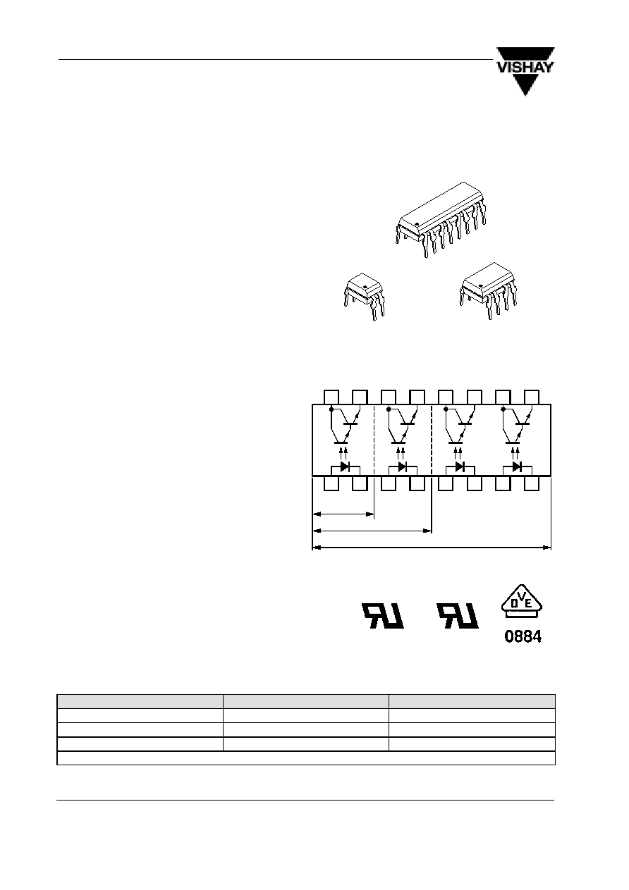
14925
Coll. Emitter
Anode
Cath.
4 PIN
8 PIN
16 PIN
14580
C
Order Instruction
Ordering Code
CTR Ranking
Remarks
TCED1100/ TCED1100G
1)
600%
4 Pin = Single channel
TCED2100
600%
8 Pin = Dual channel
TCED4100
600%
16 Pin = Quad channel
1)
G = Leadform 10.16 mm; G is not market on the body
TCED1100(G) up to TCED4100
Vishay Telefunken
Rev. A3, 11≠Jan≠99
235
Features
Approvals:
D
BSI: BS EN 41003, BS EN 60095 (BS 415),
BS EN 60950 (BS 7002),
Certificate number 7081 and 7402
D
FIMKO (SETI): EN 60950,
Certificate number 11992
D
Underwriters Laboratory (UL) 1577 recognized,
file number E-76222 ≠ Double Protection
D
CSA (C≠UL) 1577 recognized,
file number E-76222 ≠ Double Protection
D
VDE 0884, Certificate number 115667
VDE 0884 related features:
D
Rated impulse voltage (transient overvoltage)
V
IOTM
= 8 kV peak
D
Isolation test voltage
(partial discharge test voltage) V
pd
= 1.6 kV
D
Rated isolation voltage (RMS includes DC)
V
IOWM
= 600 V
RMS
(848 V peak)
D
Rated recurring peak voltage (repetitive)
V
IORM
= 600 V
RMS
D
Creepage current resistance according to
VDE 0303/IEC 112
Comparative Tracking Index: CTI
175
D
Thickness through insulation
0.75 mm
D
Internal creepage distance > 4 mm
General features:
D
Isolation materials according to UL94-VO
D
Pollution degree 2 (DIN/VDE 0110 / resp. IEC 664)
D
Climatic classification 55/100/21 (IEC 68 part 1)
D
Special construction:
Therefore, extra low coupling capacity of
typical 0.2 pF, high Common Mode Rejection
D
Low temperature coefficient of CTR
D
G = Leadform 10.16 mm;
provides creepage distance > 8 mm,
for TCED2100/ TCED4100 optional;
suffix letter `G' is not marked on the optocoupler
D
Coupling System U
Absolute Maximum Ratings
Input (Emitter)
Parameter
Test Conditions
Symbol
Value
Unit
Reverse voltage
V
R
6
V
Forward current
I
F
60
mA
Forward surge current
t
p
10
m
s
I
FSM
1.5
A
Power dissipation
T
amb
25
∞
C
P
V
100
mW
Junction temperature
T
j
125
∞
C
Output (Detector)
Parameter
Test Conditions
Symbol
Value
Unit
Collector emitter voltage
V
CEO
35
V
Emitter collector voltage
V
ECO
7
V
Collector current
I
C
80
mA
Collector peak current
t
p
/T = 0.5, t
p
10 ms
I
CM
100
mA
Power dissipation
T
amb
25
∞
C
P
V
150
mW
Junction temperature
T
j
125
∞
C
Coupler
Parameter
Test Conditions
Symbol
Value
Unit
AC isolation test voltage (RMS)
t = 1 min
V
IO
5
kV
Total power dissipation
T
amb
25
∞
C
P
tot
250
mW
Operating ambient temperature range
T
amb
≠40 to +100
∞
C
Storage temperature range
T
stg
≠55 to +125
∞
C
Soldering temperature
2 mm from case t
10 s
T
sd
260
∞
C
TCED1100(G) up to TCED4100
Vishay Telefunken
Rev. A3, 11≠Jan≠99
236
Electrical Characteristics
(T
amb
= 25
∞
C)
Input (Emitter)
Parameter
Test Conditions
Symbol
Min.
Typ.
Max.
Unit
Forward voltage
I
F
= 20 mA
V
F
1.15
1.4
V
Junction capacitance
V
R
= 0 V, f = 1 MHz
C
j
50
pF
Output (Detector)
Parameter
Test Conditions
Symbol
Min.
Typ.
Max.
Unit
Collector emitter voltage
I
C
= 1 mA
V
CEO
32
V
Emitter collector voltage
I
E
= 100
m
A
V
ECO
7
V
Collector emitter cut-off
current
V
CE
= 10 V, I
f
= 0, E = 0
I
CEO
15
100
nA
Coupler
Parameter
Test Conditions
Symbol
Min.
Typ.
Max.
Unit
Collector emitter
saturation voltage
I
F
= 20 mA, I
C
= 5 mA
V
CEsat
1
V
Cut-off frequency
V
CE
= 5 V, I
F
= 10 mA,
R
L
= 100
W
f
c
10
kHz
Coupling capacitance
f = 1 MHz
C
k
0.3
pF
Current Transfer Ratio (CTR)
Parameter
Test Conditions
Type
Symbol
Min.
Typ.
Max.
Unit
I
C
/I
F
V
CE
= 2 V, I
F
= 1 mA
TCED1100(G)/
TCED2100/
TCED4100
CTR
6.0
8.0

TCED1100(G) up to TCED4100
Vishay Telefunken
Rev. A3, 11≠Jan≠99
237
Maximum Safety Ratings
(according to VDE 0884) see figure 1
This device is used for protective separation against electrical shock only within the maximum safety ratings.
This must be ensured by using protective circuits in the applications.
Input (Emitter)
Parameters
Test Conditions
Symbol
Value
Unit
Forward current
I
si
130
mA
Output (Detector)
Parameters
Test Conditions
Symbol
Value
Unit
Power dissipation
T
amb
25
∞
C
P
si
265
mW
Coupler
Parameters
Test Conditions
Symbol
Value
Unit
Rated impulse voltage
V
IOTM
8
kV
Safety temperature
T
si
150
∞
C
Insulation Rated Parameters
(according to VDE 0884)
Parameter
Test Conditions
Symbol
Min.
Typ.
Max.
Unit
Partial discharge test voltage ≠
Routine test
100%, t
test
= 1 s
V
pd
1.6
kV
Partial discharge test voltage ≠ t
Tr
= 60 s, t
test
= 10 s,
V
IOTM
8
kV
g
g
Lot test (sample test)
Tr
test
(see figure 2)
V
pd
1.3
kV
Insulation resistance
V
IO
= 500 V
R
IO
10
12
W
V
IO
= 500 V,
T
amb
= 100
∞
C
R
IO
10
11
W
V
IO
= 500 V,
T
amb
= 150
∞
C
(construction test only)
R
IO
10
9
W
0
25
50
75
125
0
50
100
150
200
300
P
≠
T
otal Power Dissipation ( mW
)
tot
T
amb
≠ Ambient Temperature (
∞
C )
150
14887
100
250
Photodarlington
Psi ( mW )
IR-Diode
Isi ( mA )
Figure 1. Derating diagram
V
IOTM
V
Pd
V
IOWM
V
IORM
V
t
4
t
3
t
test
t
stres
t
2
t
1
t
0
13930
t
Tr
= 60 s
t
1
, t
2
= 1 to 10 s
t
3
, t
4
= 1 s
t
test
= 10 s
t
stres
= 12 s
Figure 2. Test pulse diagram for sample test according to
DIN VDE 0884

TCED1100(G) up to TCED4100
Vishay Telefunken
Rev. A3, 11≠Jan≠99
238
Switching Characteristics
Parameter
Test Conditions
Symbol
Typ.
Unit
Rise time
V
CC
= 2 V, I
C
= 10 mA, R
L
= 100
W
(see figure 3)
t
r
300
m
s
Fall time
CC
C
L
(
g
)
t
f
250
m
s
C
I
w
Channel I
Channel II
50
W
+ V
CC
Oscilloscope
R
I
w
1 M
W
20 pF
I
C
= 10 mA ;
Adjusted through
input amplitude
I
F
R
G
= 50
W
t
1
= 1 ms
0
14779
R
L
t
p
T +
0.01
I
F
Figure 3. Test circuit
t
p
t
t
0
0
10%
90%
100%
t
r
t
d
t
on
t
s
t
f
t
off
I
F
I
C
96 11698
t
p
pulse dura-
tion
t
d
delay time
t
r
rise time
t
on
(= t
d
+ t
r
)
turn-on time
t
s
storage time
t
f
fall time
t
off
(= t
s
+ t
f
)
turn-off time
Figure 4. Switching times