 | –≠–ª–µ–∫—Ç—Ä–æ–Ω–Ω—ã–π –∫–æ–º–ø–æ–Ω–µ–Ω—Ç: TCLT1109 | –°–∫–∞—á–∞—Ç—å:  PDF PDF  ZIP ZIP |
TCLT11.. Series
Document Number 83514
Rev. 1.8, 03-Dec-04
Vishay Semiconductors
www.vishay.com
1
C
17296
5
4
3
1
2
V
D E
Pb
Pb-free
e3
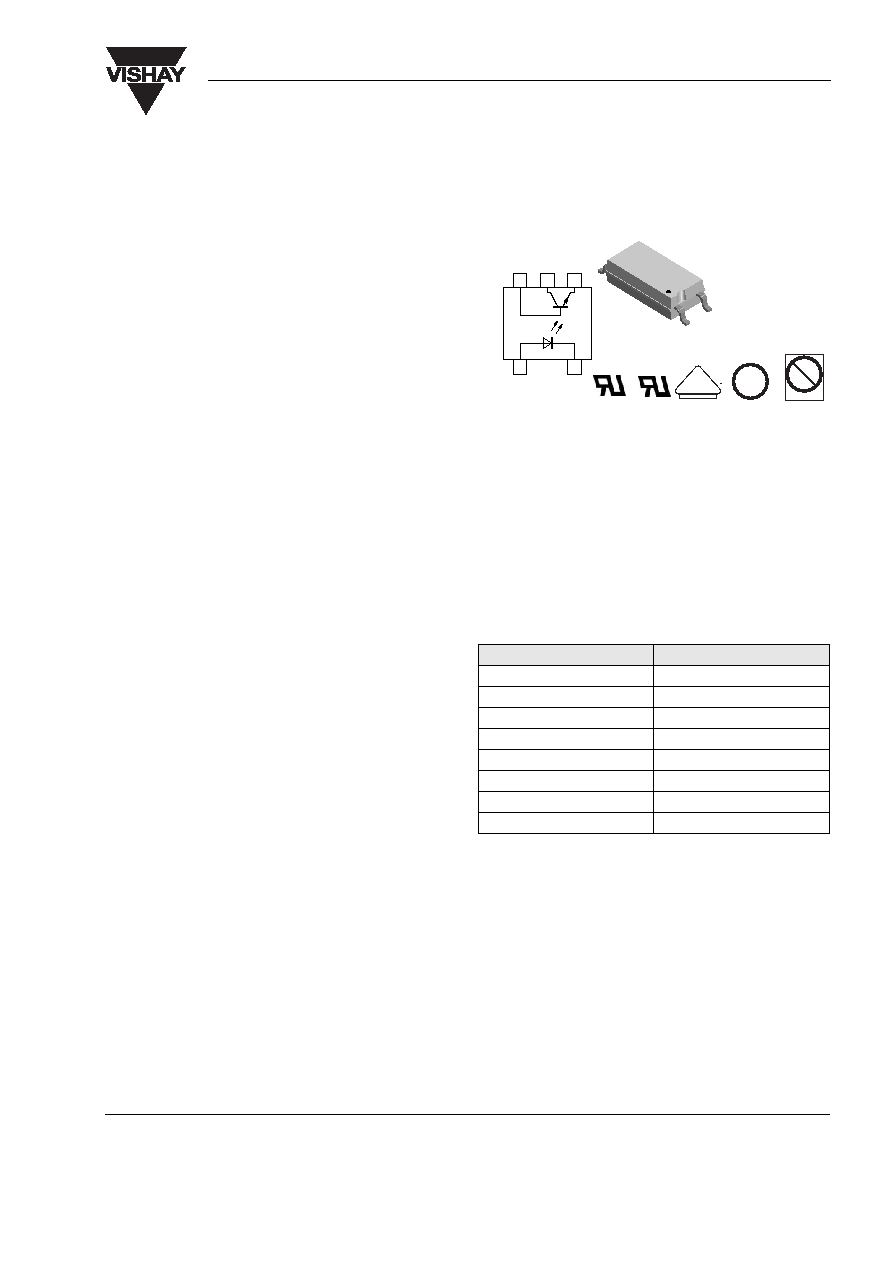
Optocoupler, Phototransistor Output, SOP-6L5, Half Pitch, Long
Mini-Flat Package
Features
∑ SMD Low profile 5 pin package
∑ Isolation Test Voltage 5000 V
RMS
∑ CTR flexibility available see order information
∑ Special construction
∑ Extra low coupling capacitance
∑ Connected base
∑ DC input with transistor output
∑ Lead-free component
∑ Component in accordance to RoHS 2002/95/EC
and WEEE 2002/96/EC
Agency Approvals
∑ UL1577, File No. E76222 System Code W, Double
Protection
∑ CSA 93751
∑ BSI IEC60950 IEC60065
∑ DIN EN 60747-5-2 (VDE0884)
DIN EN 60747-5-5 pending
∑ FIMKO
∑ NOTE:
See the Safety Standard Approval List "Agency
Table" for more detailed information.
Applications
Switchmode power supplies
Computer peripheral interface
Microprocessor system interface
Description
The TCLT11.. Series consists of a phototransistor
optically coupled to a gallium arsenide infrared-emit-
ting diode in a 5-lead SOP5L package.
The elements are mounted on one leadframe provid-
ing a fixed distance between input and output for high-
est safety requirements.
Order Information
NOTE: Available only on tape and reel.
Part
Remarks
TCLT1100
CTR 50 - 600 %, SMD-5
TCLT1102
CTR 63 - 125 %, SMD-5
TCLT1103
CTR 100 - 200 %, SMD-5
TCLT1105
CTR 50 - 150 %, SMD-5
TCLT1106
CTR 100 - 300 %, SMD-5
TCLT1107
CTR 80 - 160 %, SMD-5
TCLT1108
CTR 130 - 260 %, SMD-5
TCLT1109
CTR 200 - 400 %, SMD-5
www.vishay.com
2
Document Number 83514
Rev. 1.8, 03-Dec-04
TCLT11.. Series
Vishay Semiconductors
Absolute Maximum Ratings
T
amb
= 25 ∞C, unless otherwise specified
Stresses in excess of the absolute Maximum Ratings can cause permanent damage to the device. Functional operation of the device is
not implied at these or any other conditions in excess of those given in the operational sections of this document. Exposure to absolute
Maximum Rating for extended periods of the time can adversely affect reliability.
Input
Output
Coupler
Electrical Characteristics
T
amb
= 25 ∞C, unless otherwise specified
Minimum and maximum values are testing requirements. Typical values are characteristics of the device and are the result of engineering
evaluation. Typical values are for information only and are not part of the testing requirements.
Input
Output
Parameter
Test condition
Symbol
Value
Unit
Reverse voltage
V
R
6
V
Forward current
I
F
60
mA
Forward surge current
t
p
10 µs
I
FSM
1.5
A
Power dissipation
P
diss
100
mW
Junction temperature
T
j
125
∞C
Parameter
Test condition
Symbol
Value
Unit
Collector emitter voltage
V
CEO
70
V
Emitter collector voltage
V
ECO
7
V
Collector current
I
C
50
mA
Collector peak current
t
p
/T = 0.5, t
p
10 ms
I
CM
100
mA
Power dissipation
P
diss
150
mW
Junction temperature
T
j
125
∞C
Parameter
Test condition
Symbol
Value
Unit
Isolation test voltage (RMS)
V
ISO
5000
V
RMS
Total power dissipation
P
tot
250
mW
Operating ambient temperature
range
T
amb
- 40 to + 100
∞C
Storage temperature range
T
stg
- 40 to + 100
∞C
Soldering temperature
T
sld
240
∞C
Parameter
Test condition
Symbol
Min
Typ.
Max
Unit
Forward voltage
I
F
= ± 50 mA
V
F
1.25
1.6
V
Junction capacitance
V
R
= 0 V, f = 1 MHz
C
j
50
pF
Parameter
Test condition
Symbol
Min
Typ.
Max
Unit
Collector emitter voltage
I
C
= 1 mA
V
CEO
70
V
Emitter collector voltage
I
E
= 100
µA
V
ECO
7
V
Collector-emitter cut-off current
V
CE
= 20 V, I
f
= 0, E = 0
I
CEO
10
100
nA
TCLT11.. Series
Document Number 83514
Rev. 1.8, 03-Dec-04
Vishay Semiconductors
www.vishay.com
3
Coupler
Current Transfer Ratio
Maximum Safety Ratings
(according to DIN EN 60747-5-2(VDE0884)/ DIN EN 60747-5-5 pending) see figure 1
This optocoupler is suitable for safe electrical isolation only within the safety ratings.
Compliance with the safety ratings shall be ensured by means of suitable protective circuits.
Input
Output
Coupler
Parameter
Test condition
Symbol
Min
Typ.
Max
Unit
Collector emitter saturation
voltage
I
F
= 10 mA, I
C
= 1 mA
V
CEsat
0.3
V
Cut-off frequency
V
CE
= 5 V, I
F
= 10 mA,
R
L
= 100
f
c
110
kHz
Coupling capacitance
f = 1 MHz
C
k
0.3
pF
Parameter
Test condition
Part
Symbol
Min
Typ.
Max
Unit
I
C
/I
F
V
CE
= 5 V, I
F
= 5 mA
TCLT1100
CTR
50
600
%
V
CE
= 5 V, I
F
= 10 mA
TCLT1102
CTR
63
125
%
TCLT1103
CTR
100
200
%
V
CE
= 5 V, I
F
= 1 mA
TCLT1102
CTR
22
45
%
TCLT1103
CTR
34
70
%
TCLT1104
CTR
56
100
%
V
CE
= 5 V, I
F
= 5 mA
TCLT1105
CTR
50
150
%
TCLT1106
CTR
100
300
%
TCLT1107
CTR
80
160
%
TCLT1108
CTR
130
260
%
TCLT1109
CTR
200
400
%
Parameter
Test condition
Symbol
Min
Typ.
Max
Unit
Forward current
I
F
130
mA
Parameter
Test condition
Symbol
Min
Typ.
Max
Unit
Power dissipation
P
diss
265
mW
Parameter
Test condition
Symbol
Min
Typ.
Max
Unit
Rated impulse voltage
V
IOTM
8
kV
Safety temperature
T
si
150
∞C

www.vishay.com
4
Document Number 83514
Rev. 1.8, 03-Dec-04
TCLT11.. Series
Vishay Semiconductors
Insulation Rated Parameters
Parameter
Test condition
Symbol
Min
Typ.
Max
Unit
Partial discharge test voltage -
Routine test
100 %, t
test
= 1 s
V
pd
1.6
kV
Partial discharge test voltage -
Lot test (sample test)
t
Tr
= 60 s, t
test
= 10 s,
(see figure 2)
V
IOTM
8
kV
V
pd
1.3
kV
Insulation resistance
V
IO
= 500 V
R
IO
10
12
V
IO
= 500 V, T
amb
= 100 ∞C
R
IO
10
11
V
IO
= 500 V, T
amb
= 150 ∞C
(construction test only)
R
IO
10
9
Figure 1. Derating diagram
4.8
4.4
1.40
1.27
10 4
3 8
Figure 2. Test pulse diagram for sample test according to DIN EN
60747-5-2(VDE0884)/ DIN EN 60747-; IEC60747
t
13930
t
1
, t
2
= 1 to 10 s
t
3
, t
4
= 1 s
t
test
= 10 s
t
stres
= 12 s
V
IOTM
V
Pd
V
IOWM
V
IORM
0
t
1
t
test
t
Tr
= 60 s
t
stres
t
3
t
4
t
2
TCLT11.. Series
Document Number 83514
Rev. 1.8, 03-Dec-04
Vishay Semiconductors
www.vishay.com
5
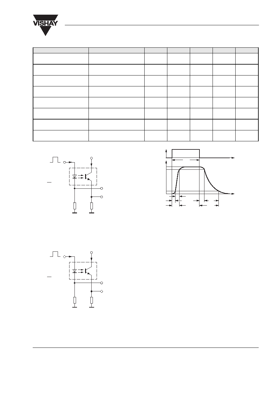
Switching Characteristics
Parameter
Test condition
Symbol
Min
Typ.
Max
Unit
Delay time
V
S
= 5 V, I
C
= 2 mA, R
L
= 100
(see figure 3)
t
d
3.0
µs
Rise time
V
S
= 5 V, I
C
= 2 mA, R
L
= 100
(see figure 3)
t
r
3.0
µs
Turn-on time
V
S
= 5 V, I
C
= 2 mA, R
L
= 100
(see figure 3)
t
on
6.0
µs
Storage time
V
S
= 5 V, I
C
= 2 mA, R
L
= 100
(see figure 3)
t
s
0.3
µs
Fall time
V
S
= 5 V, I
C
= 2 mA, R
L
= 100
(see figure 3)
t
f
4.7
µs
Turn-off time
V
S
= 5 V, I
C
= 2 mA, R
L
= 100
(see figure 3)
t
off
5.0
µs
Turn-on time
V
S
= 5 V, I
F
= 10 mA, R
L
= 1 k
(see figure 4)
t
on
9.0
µs
Turn-off time
V
S
= 5 V, I
F
= 10 mA, R
L
= 1 k
(see figure 4)
t
off
10.0
µs
Figure 3. Test circuit, non-saturated operation
Figure 4. Test circuit, saturated operation
Channel I
Channel II
95 10804
R
G
= 50
W
t
p
t
p
= 50 s
T
= 0.01
+ 5 V
I
F
0
50
W
100
W
I
F
I
C
= 2 mA; adjusted through
input amplitude
Oscilloscope
R
L
= 1 M
W
C
L
= 20 pF
Channel I
Channel II
95 10843
R
G
= 50
t
p
t
p
= 50 s
T
= 0.01
+ 5 V
I
C
I
F
0
50
1 k
I
F
= 10 mA
Oscilloscope
R
L
C
L
20 pF
M
1
µ
Figure 5. Switching Times
t
p
t
t
0
0
10%
90%
100%
t
r
t
d
t
on
t
s
t
f
t
off
I
F
I
C
96 11698
t
p
pulse duration
t
d
delay time
t
r
rise time
t
on
(= t
d
+ t
r
)
turn-on time
t
s
storage time
t
f
fall time
t
off
(= t
s
+ t
f
)
turn-off time