 | ÐлекÑÑоннÑй компоненÑ: TLCY5100 | СкаÑаÑÑ:  PDF PDF  ZIP ZIP |
Äîêóìåíòàöèÿ è îïèñàíèÿ www.docs.chipfind.ru
TLCB / R / TG / Y5100
Document Number 83176
Rev. 1.4, 16-Feb-05
Vishay Semiconductors
www.vishay.com
1
19223
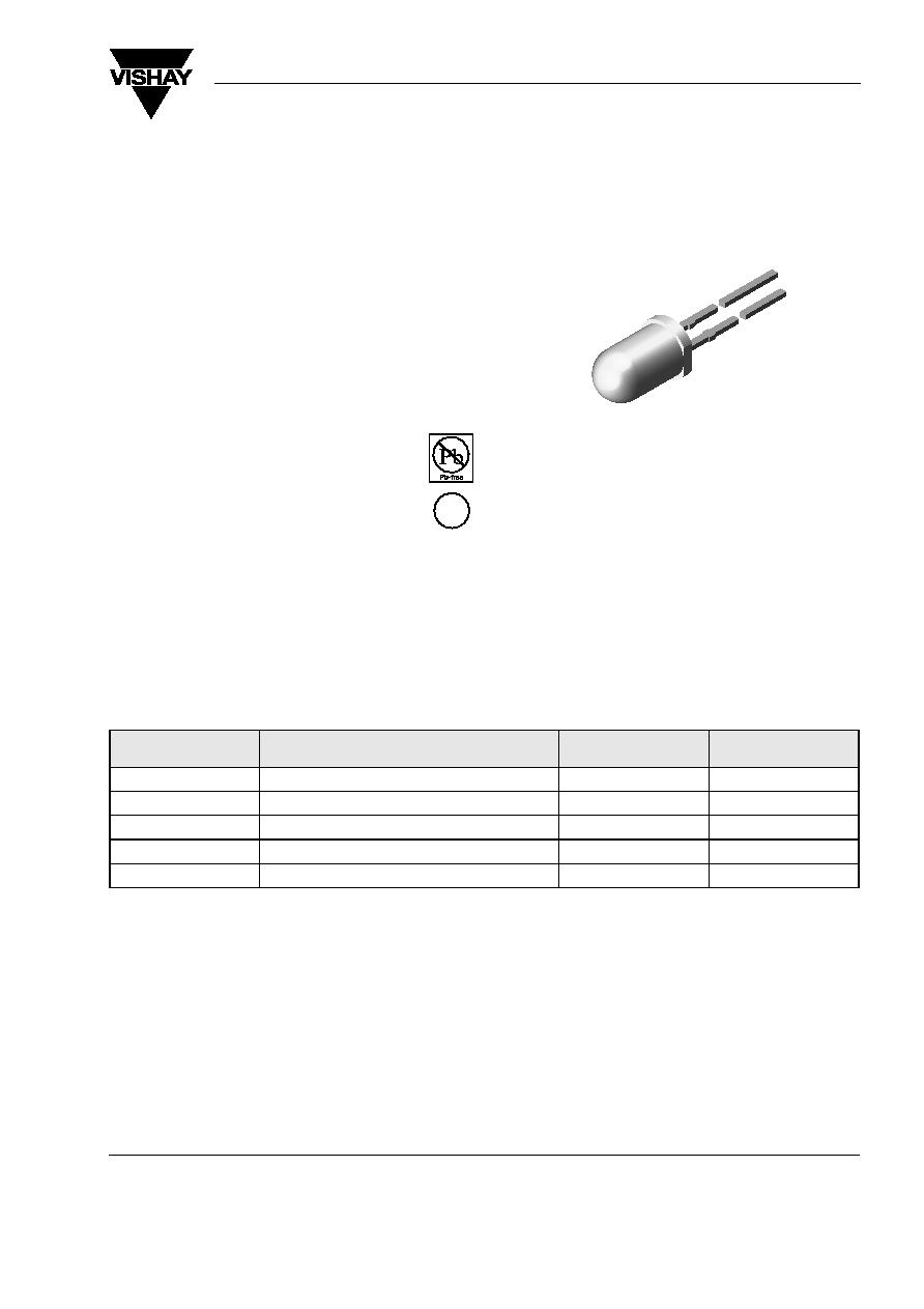
Ultrabright LED,
5 mm Untinted Non-Diffused
Description
The TLC.51.. series is a clear, non diffused 5 mm LED
for high end applications where supreme luminous
intensity required.
These lamps with clear untinted plastic case utilize
the highly developed ultrabright AlInGaP (AS) and
InGaN technologies.
The lens and the viewing angle is optimized to
achieve best performance of light output and visibility.
Features
· Untinted non diffused lens
· Utilizing ultrabright AllnGaP (AS) and
InGaN technology
· High luminous intensity
· High operating tempreature: T
j
(chip junction tem-
perature) up to 125 °C for AllnGaP devices
· Luminous intensity and color categorized for each
packing unit
· ESD-withstand voltage: 2 kV acc. to MIL STD 883
D, Method 3015.7 for AllnGaP, 1 kV for InGaN
· Lead-free device
Applications
Interior and exterior lighting
Outdoor LED panels
Instrumentation and front panel indicators
Central high mounted stop lights (CHMSL) for motor
vehicles
Replaces incandescent lamps
Traffic signals
Light guide design
Parts Table
Part
Color, Luminous Intensity
Angle of Half Intensity
(±
)
Technology
TLCR5100
Red, I
V
> 11000 mcd (typ.)
9 °
AllnGaP on GaAs
TLCY5100
Yellow, I
V
> 7500 mcd (typ.)
9 °
AllnGaP on GaAs
TLCY5101
Yellow, I
V
> 5750 mcd to 20000 mcd
9 °
AllnGaP on GaAs
TLCTG5100
True green, I
V
> 5000 mcd (typ.)
9 °
InGaN on SiC
TLCB5100
Blue, I
V
> 1500 mcd (typ.)
9 °
InGaN on SiC
e2
www.vishay.com
2
Document Number 83176
Rev. 1.4, 16-Feb-05
TLCB / R / TG / Y5100
Vishay Semiconductors
Absolute Maximum Ratings
T
amb
= 25 °C, unless otherwise specified
TLCR5100 , TLCY5100
TLCTG5100 , TLCB5100
Optical and Electrical Characteristics
T
amb
= 25 °C, unless otherwise specified
Red
TLCR5100
1)
in one Packing Unit I
Vmax
/I
Vmin
2.0
Parameter
Test condition
Symbol
Value
Unit
Reverse voltage
V
R
5
V
DC Forward current
T
amb
85 °C
I
F
50
mA
Surge forward current
t
p
10
µ
s
I
FSM
1
A
Power dissipation
T
amb
85 °C
P
V
135
mW
Junction temperature
T
j
125
°C
Operating temperature range
T
amb
- 40 to + 100
°C
Storage temperature range
T
stg
- 40 to + 100
°C
Soldering temperature
t
5 s, 2 mm from body
T
sd
260
°C
Thermal resistance junction/
ambient
R
thJA
300
K/W
Parameter
Test condition
Symbol
Value
Unit
Reverse voltage
V
R
5
V
DC Forward current
T
amb
60 °C
I
F
30
mA
Surge forward current
t
p
10
µ
s
I
FSM
0.1
A
Power dissipation
T
amb
60 °C
P
V
135
mW
Junction temperature
T
j
100
°C
Operating temperature range
T
amb
- 40 to + 100
°C
Storage temperature range
T
stg
- 40 to + 100
°C
Soldering temperature
t
5 s, 2 mm from body
T
sd
260
°C
Thermal resistance junction/
ambient
R
thJA
300
K/W
Parameter
Test condition
Part
Symbol
Min
Typ.
Max
Unit
Luminous intensity
1)
I
F
= 50 mA
TLCR5100
I
V
4300
11000
mcd
Dominant wavelength
I
F
= 50 mA
d
611
616
622
nm
Peak wavelength
I
F
= 50 mA
p
622
nm
Spectral bandwidth at
50 % I
rel max
I
F
= 50 mA
18
nm
Angle of half intensity
I
F
= 50 mA
± 9
deg
Forward voltage
I
F
= 50 mA
V
F
2.1
2.7
V
Reverse voltage
I
R
= 10
µ
A
V
R
5
V
Temperature coefficient of V
F
I
F
= 50 mA
TC
VF
- 3.5
mV/K
Temperature coefficient of
d
I
F
= 50 mA
TC
d
0.05
nm/K
TLCB / R / TG / Y5100
Document Number 83176
Rev. 1.4, 16-Feb-05
Vishay Semiconductors
www.vishay.com
3
Yellow
TLCY5100
1)
in one Packing Unit I
Vmax
/I
Vmin
2.0
True green
TLCTG5100
1)
in one Packing Unit I
Vmax
/I
Vmin
2.0
Blue
TLCB5100
1)
in one Packing Unit I
Vmax
/I
Vmin
2.0
Parameter
Test condition
Part
Symbol
Min
Typ.
Max
Unit
Luminous intensity
1)
I
F
= 50 mA
TLCY5100
I
V
3200
7500
mcd
TLCY5101
I
V
6900
16000
mcd
Dominant wavelength
I
F
= 50 mA
d
585
590
597
nm
Peak wavelength
I
F
= 50 mA
p
593
nm
Spectral bandwidth at
50 % I
rel max
I
F
= 50 mA
17
nm
Angle of half intensity
I
F
= 50 mA
± 9
deg
Forward voltage
I
F
= 50 mA
V
F
2.1
2.7
V
Reverse voltage
I
R
= 10
µ
A
V
R
5
V
Temperature coefficient of V
F
I
F
= 50 mA
TC
VF
- 3.5
mV/K
Temperature coefficient of
d
I
F
= 50 mA
TC
d
0.1
nm/K
Parameter
Test condition
Part
Symbol
Min
Typ.
Max
Unit
Luminous intensity
1)
I
F
= 30 mA
TLCTG5100
I
V
1800
5000
mcd
Dominant wavelength
I
F
= 30 mA
d
515
525
535
nm
Peak wavelength
I
F
= 30 mA
p
520
nm
Spectral bandwidth at
50 % I
rel max
I
F
= 30 mA
37
nm
Angle of half intensity
I
F
= 30 mA
± 9
deg
Forward voltage
I
F
= 30 mA
V
F
3.9
4.5
V
Reverse voltage
I
R
= 10
µ
A
V
R
5
V
Temperature coefficient of V
F
I
F
= 30 mA
TC
VF
- 4.5
mV/K
Temperature coefficient of
d
I
F
= 30 mA
TC
d
0.02
nm/K
Parameter
Test condition
Part
Symbol
Min
Typ.
Max
Unit
Luminous intensity
1)
I
F
= 30 mA
TLCB5100
I
V
575
1500
mcd
Dominant wavelength
I
F
= 30 mA
d
462
470
476
nm
Peak wavelength
I
F
= 30 mA
p
464
nm
Spectral bandwidth at
50 % I
rel max
I
F
= 30 mA
25
nm
Angle of half intensity
I
F
= 30 mA
± 9
deg
Forward voltage
I
F
= 30 mA
V
F
3.9
4.5
V
Reverse voltage
I
R
= 10
µ
A
V
R
5
V
Temperature coefficient of V
F
I
F
= 30 mA
TC
VF
- 5.0
mV/K
Temperature coefficient of
d
I
F
= 30 mA
TC
d
0.02
nm/K
www.vishay.com
4
Document Number 83176
Rev. 1.4, 16-Feb-05
TLCB / R / TG / Y5100
Vishay Semiconductors
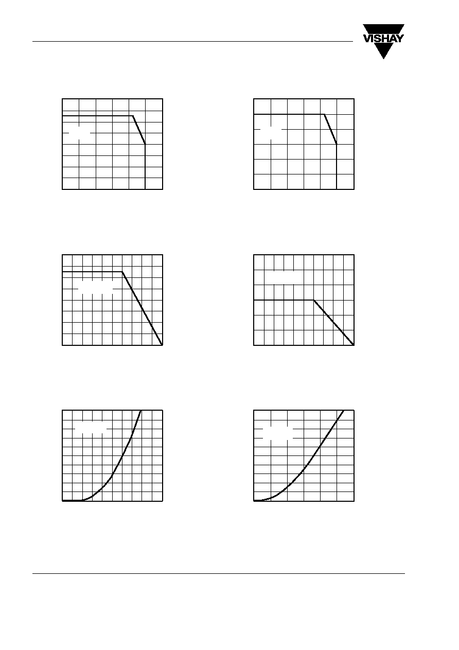
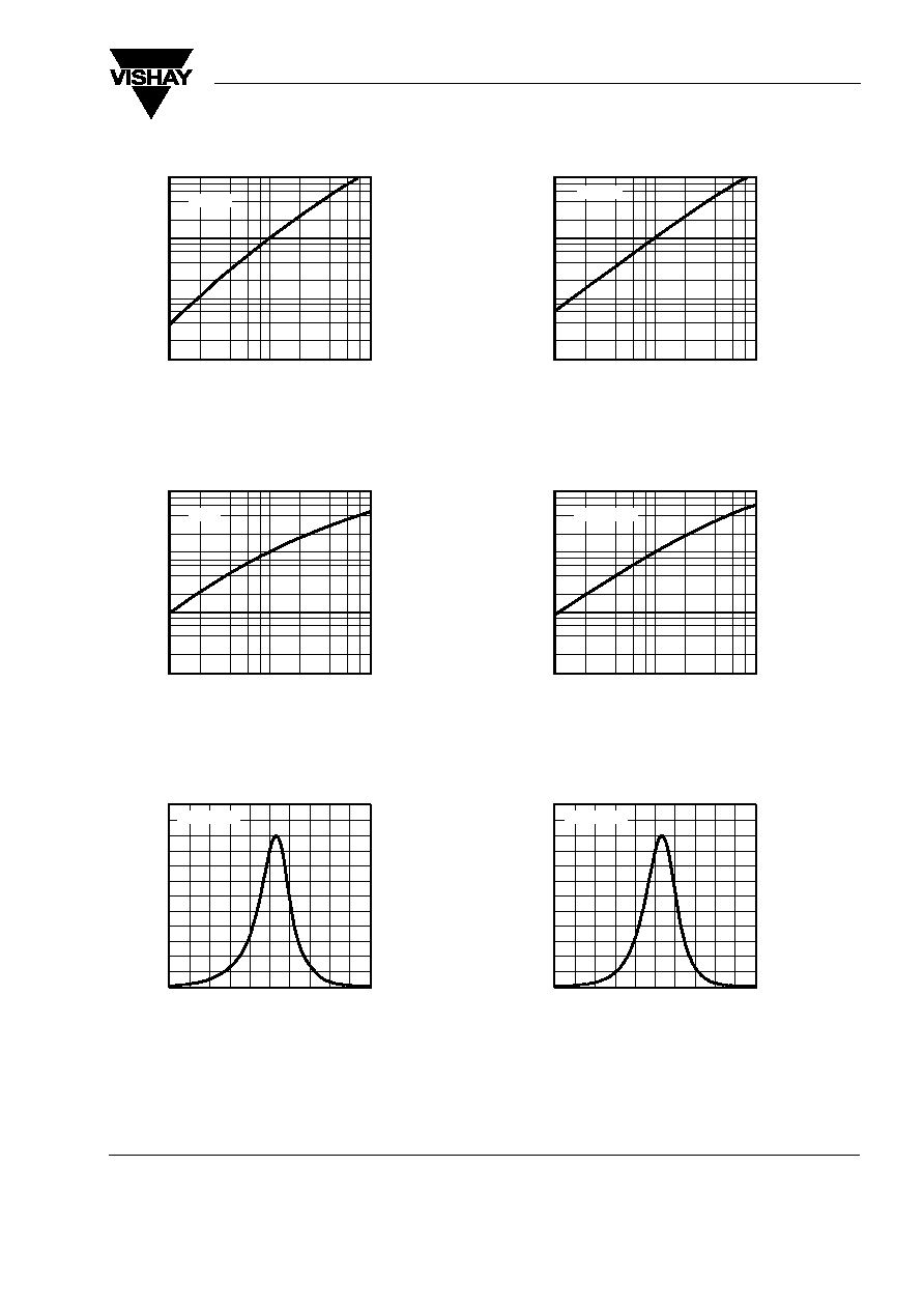
Typical Characteristics (Tamb = 25
°C unless otherwise specified)
Figure 1. Power Dissipation vs. Ambient Temperature
Figure 2. Power Dissipation vs. Ambient Temperature
Figure 3. Forward Current vs. Forward Voltage
0
20
40
60
80
100
120
140
160
0
20
40
60
80
100
120
T
amb
Ambient Temperature (
°C )
16708
P
Power
Dissipation
(mW)
V
Yellow
Red
0
20
40
60
80
100
120
140
160
0
10 20 30 40 50 60 70 80 90 100
T
amb
Ambient Temperature (
°
C )
16709
P
Power Dissipation (mW)
V
Blue
Truegreen
0
10
20
30
40
50
60
70
80
90
100
1.5 1.6 1.7 1.8 1.9 2.0 2.1 2.2 2.3 2.4 2.5
V
F
Forward Voltage ( V )
15974
F
I
F
orward
Current
(
m
A
)
Red
Yellow
Figure 4. Forward Current vs. Ambient Temperature
Figure 5. Forward Current vs. Ambient Temperature
Figure 6. Forward Current vs. Forward Voltage
0
10
20
30
40
50
60
0
20
40
60
80
100
120
T
amb
Ambient Temperature (
°
C )
16710
Yellow
Red
I Forward Current ( mA
)
F
0
10
20
30
40
50
60
0
10 20 30 40 50 60 70 80 90 100
T
amb
Ambient Temperature (
°
C )
16711
Blue
Truegreen
I Forward Current ( mA
)
F
0
10
20
30
40
50
60
70
80
90
100
2.5
3.0
3.5
4.0
4.5
5.0
5.5
V
F
- Forward Voltage ( V )
16040
Blue
Truegreen
I
-
Forward
Current
(
m
A
)
F
TLCB / R / TG / Y5100
Document Number 83176
Rev. 1.4, 16-Feb-05
Vishay Semiconductors
www.vishay.com
5
Figure 7. Relative Luminous Flux vs. Forward Current
Figure 8. Relative Luminous Flux vs. Forward Current
Figure 9. Relative Intensity vs. Wavelength
0.01
0.1
1
10
1
10
100
I
F
- Forward Current ( mA )
15978
I
-
Relative
Luminous
Intensity
Vrel
Red
0.01
0.10
1.00
10.00
1
10
100
I
F
- Forward Current ( mA )
16042
Blue
Vrel
I
-
Relative
Luminous
Intensity
0.0
0.1
0.2
0.3
0.4
0.5
0.6
0.7
0.8
0.9
1.0
1.1
1.2
570 580 590 600 610 620 630 640 650 660 670
- Wavelength ( nm )
16007
I
-
Relative
Luminous
Intensity
Vrel
Red
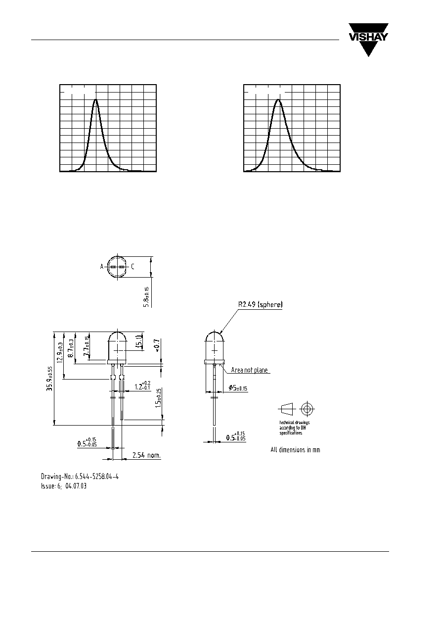
Figure 10. Relative Luminous Flux vs. Forward Current
Figure 11. Relative Luminous Flux vs. Forward Current
Figure 12. Relative Intensity vs. Wavelength
V
rel
0.01
0.1
1
10
1
10
100
I
F
- Forward Current ( mA )
15979
Yellow
I
-
Relative
Luminous
Intensity
0.01
0.10
1.00
10.00
1
10
100
I
F
- Forward Current ( mA )
16039
True Green
Vrel
I
-
Relative
Luminous
Intensity
0.0
0.1
0.2
0.3
0.4
0.5
0.6
0.7
0.8
0.9
1.0
1.1
1.2
540 550 560 570 580 590 600 610 620 630 640
- Wavelength ( nm )
16008
I
-
Relative
Luminous
Intensity
V
rel
Yellow
www.vishay.com
6
Document Number 83176
Rev. 1.4, 16-Feb-05
TLCB / R / TG / Y5100
Vishay Semiconductors
Package Dimensions in mm
Figure 13. Relative Intensity vs. Wavelength
0.0
0.1
0.2
0.3
0.4
0.5
0.6
0.7
0.8
0.9
1.0
1.1
1.2
400 420 440 460 480 500 520 540 560
- W avelength ( nm )
16069
I
-
Relative
Luminous
Intensity
Vrel
Blue
Figure 14. Relative Intensity vs. Wavelength
0.0
0.1
0.2
0.3
0.4
0.5
0.6
0.7
0.8
0.9
1.0
1.1
1.2
460 480 500 520 540 560 580 600 620
- Wavelength ( nm )
16068
I
-
Relative
Luminous
Intensity
Vrel
True Green
9612121

TLCB / R / TG / Y5100
Document Number 83176
Rev. 1.4, 16-Feb-05
Vishay Semiconductors
www.vishay.com
7
Ozone Depleting Substances Policy Statement
It is the policy of Vishay Semiconductor GmbH to
1. Meet all present and future national and international statutory requirements.
2. Regularly and continuously improve the performance of our products, processes, distribution and
operatingsystems with respect to their impact on the health and safety of our employees and the public, as
well as their impact on the environment.
It is particular concern to control or eliminate releases of those substances into the atmosphere which are
known as ozone depleting substances (ODSs).
The Montreal Protocol (1987) and its London Amendments (1990) intend to severely restrict the use of ODSs
and forbid their use within the next ten years. Various national and international initiatives are pressing for an
earlier ban on these substances.
Vishay Semiconductor GmbH has been able to use its policy of continuous improvements to eliminate the use
of ODSs listed in the following documents.
1. Annex A, B and list of transitional substances of the Montreal Protocol and the London Amendments
respectively
2. Class I and II ozone depleting substances in the Clean Air Act Amendments of 1990 by the Environmental
Protection Agency (EPA) in the USA
3. Council Decision 88/540/EEC and 91/690/EEC Annex A, B and C (transitional substances) respectively.
Vishay Semiconductor GmbH can certify that our semiconductors are not manufactured with ozone depleting
substances and do not contain such substances.
We reserve the right to make changes to improve technical design
and may do so without further notice.
Parameters can vary in different applications. All operating parameters must be validated for each
customer application by the customer. Should the buyer use Vishay Semiconductors products for any
unintended or unauthorized application, the buyer shall indemnify Vishay Semiconductors against all
claims, costs, damages, and expenses, arising out of, directly or indirectly, any claim of personal
damage, injury or death associated with such unintended or unauthorized use.
Vishay Semiconductor GmbH, P.O.B. 3535, D-74025 Heilbronn, Germany
Telephone: 49 (0)7131 67 2831, Fax number: 49 (0)7131 67 2423