
TSOP18..ST1
Vishay Telefunken
1 (6)
Rev. 1, 08-Mar-00
www.vishay.de
∑
FaxBack +1-408-970-5600
Document Number 82106
Photo Modules for PCM Remote Control Systems
Available types for different carrier frequencies
Type
fo
Type
fo
TSOP1830ST1
30 kHz
TSOP1833ST1
33 kHz
TSOP1836ST1
36 kHz
TSOP1837ST1
36.7 kHz
TSOP1838ST1
38 kHz
TSOP1840ST1
40 kHz
TSOP1856ST1
56 kHz
Description
The TSOP18..ST1 ≠ series are miniaturized receivers
for infrared remote control systems. PIN diode and
preamplifier are assembled on lead frame, the epoxy
package is designed as IR filter.
The demodulated output signal can directly be de-
coded by a microprocessor. The main benefit is the
reliable function even in disturbed ambient and the
protection against uncontrolled output pulses.
16123
Features
D
Photo detector and preamplifier in one package
D
Internal filter for PCM frequency
D
TTL and CMOS compatibility
D
Output active low
D
Improved shielding against electrical field distur-
bance
D
Suitable burst length
6 cycles/burst
Special Features
D
Small size package
D
Enhanced immunity against all kinds of distur-
bance light
D
No occurrence of disturbance pulses at the out-
put
D
Short settling time after power on (<200
m
s)
Block Diagram
9612226
PIN
Input
AGC
Control
Circuit
Band
Pass
Demodu-
lator
30 k
W
2
3
1
V
S
OUT
GND

TSOP18..ST1
Vishay Telefunken
Rev. 1, 08-Mar-00
www.vishay.de
∑
FaxBack +1-408-970-5600
Document Number 82106
2 (6)
Absolute Maximum Ratings
T
amb
= 25
_
C
Parameter
Test Conditions
Symbol
Value
Unit
Supply Voltage
(Pin 3)
V
S
≠0.3...6.0
V
Supply Current
(Pin 3)
I
S
5
mA
Output Voltage
(Pin 1)
V
O
≠0.3...6.0
V
Output Current
(Pin 1)
I
O
5
mA
Junction Temperature
T
j
100
∞
C
Storage Temperature Range
T
stg
≠25...+85
∞
C
Operating Temperature Range
T
amb
≠25...+85
∞
C
Power Consumption
(T
amb
x
85
∞
C)
P
tot
50
mW
Soldering Temperature
t
x
10 s, 1 mm from case
T
sd
260
∞
C
Basic Characteristics
T
amb
= 25
_
C
Parameter
Test Conditions
Symbol
Min
Typ
Max
Unit
Supply Current (Pin 3)
V
S
= 5 V, E
v
= 0
I
SD
0.9
1.2
1.5
mA
y
(
)
V
S
= 5 V, E
v
= 40 klx, sunlight
I
SH
1.3
mA
Supply Voltage (Pin 3)
V
S
4.5
5.5
V
Transmission Distance
E
v
= 0, test signal see fig.6, IR diode
TSAL6200, I
F
= 300 mA
d
35
m
Output Voltage Low (Pin 1)
I
OSL
= 0.5 mA,E
e
= 0.7 mW/m
2
, f = f
o
V
OSL
250
mV
Irradiance (30 ≠ 40 kHz)
Pulse width tolerance: t
pi
≠ 4/f
o
< t
po
<
t
pi
+ 6/f
o
, test signal see fig.6
E
e min
0.3
0.5
mW/m
2
Irradiance (56 kHz)
Pulse width tolerance: t
pi
≠ 4/f
o
< t
po
<
t
pi
+ 6/f
o
, test signal see fig.6
E
e min
0.4
0.7
mW/m
2
Irradiance
E
e max
30
W/m
2
Directivity
Angle of half transmission distance
1/2
±
45
deg
Application Circuit
16179
TSAL62..
TSOP18..ST1
3
1
2
4.7
m
F
*)
m
C
>10 k
W
optional
100
W
*)
+ 5 V **)
*)
recommended to suppress power supply disturbances
GND
TSOP18..ST1
Vishay Telefunken
3 (6)
Rev. 1, 08-Mar-00
www.vishay.de
∑
FaxBack +1-408-970-5600
Document Number 82106
Typical Characteristics (T
amb
= 25
_
C unless otherwise specified)
0.7
0.8
0.9
1.0
1.1
E / E ≠ Rel. Responsitivity
e min
f / f
0
≠ Relative Frequency
1.3
94 9102
0.0
0.2
0.4
0.6
0.8
1.0
e
1.2
f = f
0
"5%
Df ( 3dB ) = f
0
/ 7
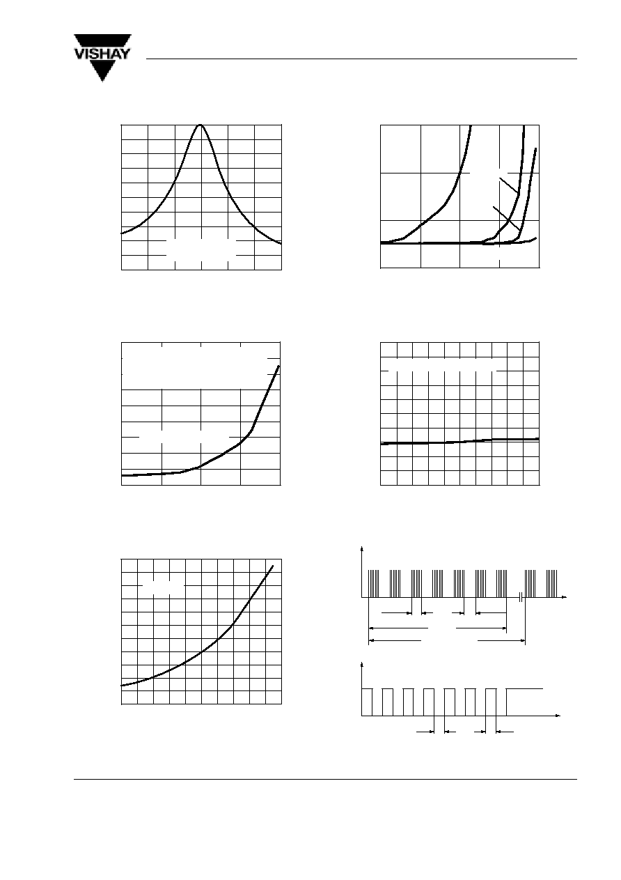
Figure 1. Frequency Dependence of Responsivity
0
0.5
1.0
1.5
2.0
2.5
3.0
3.5
4.0
4.5
0.01
0.10
1.00
10.00
100.00
E ≠ DC Irradiance (W/m
2
)
96 12214
e min
E ≠
Threshold
Irradiance
(mW/m
)
2
Correlation with ambient light sources
( Disturbance effect ) : 1 0W/m2
^1.4 klx
( Stand.illum.A, T = 2855 K )
^8.2 klx
( Daylight, T = 5900 K )
Ambient,
l = 950 nm
Figure 2. Sensitivity in Bright Ambient
0.0
0.4
0.8
1.2
1.6
0.0
0.4
0.8
1.2
2.0
E ≠ Field Strength of Disturbance ( kV / m )
2.0
94 8147
1.6
E ≠
Threshold Irradiance ( mW/m )
e min
2
f ( E ) = f
0
Figure 3. Sensitivity vs. Electric Field Disturbances
0.1
1.0
10.0
100.0
0.1
1.0
10.0
100.0
1000.0
DV
s RMS ≠
AC Voltage on DC Supply Voltage (mV)
96 12215
e min
E ≠
Threshold
Irradiance
(mW/m
)
2
f = f
o
10 kHz
1 kHz
100 Hz
Figure 4. Sensitivity vs. Supply Voltage Disturbances
0
0.1
0.2
0.3
0.4
0.5
0.6
0.7
0.8
0.9
1.0
4.5 4.6 4.7 4.8 4.9 5.0 5.1 5.2 5.3 5.4 5.5
V
S
≠ Supply Voltage ( V )
14312
e min
E ≠
Threshold
Irradiance
(mW/m
)
2
Sensitivity in dark ambient
Figure 5. Sensitivity vs. Supply Voltage
E
e
t
V
O
V
OH
V
OL
t
600
ms
600
ms
T
rep
=100 ms
T
on
T
off
9612218
Optical Test Signal
Output Signal, ( see Fig.7 )
T
D
*
* T
rep
≠T
D
> 15 ms is recommended for optimal function
Figure 6. Output Function

TSOP18..ST1
Vishay Telefunken
Rev. 1, 08-Mar-00
www.vishay.de
∑
FaxBack +1-408-970-5600
Document Number 82106
4 (6)
0.4
0.45
0.50
0.55
0.60
0.65
0.70
0.75
0.80
0.1
1.0
10.0
100.0 1000.0 10000.0100000.0
E
e
≠ Irradiance (mW/m
2
)
16163
on of
f
T
,T
≠ Output Pulse Length (ms)
T
on
optical test signal, fig.6
T
off
Figure 7. Output Pulse Diagram
0
0.2
0.4
0.6
0.8
1.0
1.2
1.4
1.6
1.8
2.0
≠30 ≠15
0
15
30
45
60
75
90
T
amb
≠ Ambient Temperature (
∞
C )
14315
I ≠ Supply Current ( mA
)
s
V
s
= 5 V
Figure 8. Supply Current vs. Ambient Temperature
0
0.1
0.2
0.3
0.4
0.5
0.6
0.7
0.8
0.9
1.0
≠30 ≠15
0
15
30
45
60
75
90
T
amb
≠ Ambient Temperature (
∞
C )
96 12221
e min
E ≠
Threshold
Irradiance
(mW/m
)
2
Sensitivity in dark ambient
Figure 9. Sensitivity vs. Ambient Temperature
0.5
0.6
0.7
0.8
0.9
1.0
1.1
1.2
1.3
1.4
1.5
1.6
1.7
4.5 4.6 4.7 4.8 4.9 5.0 5.1 5.2 5.3 5.4 5.5
V
S
≠ Supply Voltage ( V )
14317
I ≠ Supply Current ( mA
)
s
Supply current in dark ambient
Figure 10. Supply Current vs. Supply Voltage
750
850
950
1050
0
0.2
0.4
0.6
0.8
1.2
S ( ) ≠ Relative Spectral Sensitivity
rel
l ≠ Wavelength ( nm )
1150
94 8408
1.0
l
Figure 11. Relative Spectral Sensitivity vs. Wavelength
96 12223p2
0.4
0.2
0
0.2
0.4
0.6
0.6
0.9
0
∞
30
∞
10
∞
20
∞
40
∞
50
∞
60
∞
70
∞
80
∞
1.0
0.8
0.7
d
rel
≠ Relative Transmission Distance
Figure 12. Directivity
TSOP18..ST1
Vishay Telefunken
5 (6)
Rev. 1, 08-Mar-00
www.vishay.de
∑
FaxBack +1-408-970-5600
Document Number 82106
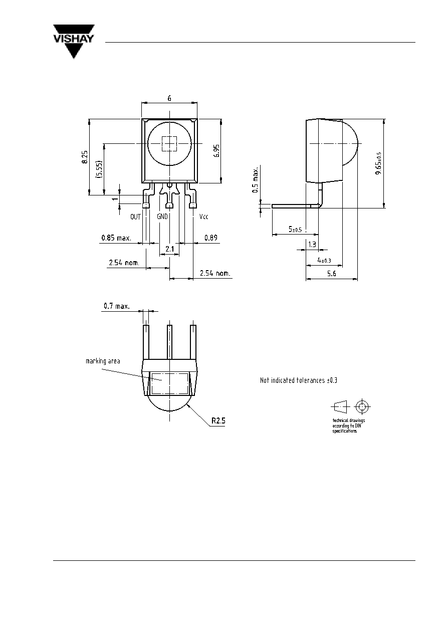
Dimensions in mm
16209