VO0600T/0601T/0611T/0630T/0631T/0661T
Document Number 84607
Rev. 1.4, 04-Jul-06
Vishay Semiconductors
www.vishay.com
1
1
2
3
4
8
7
6
5
1
2
3
4
8
7
6
5
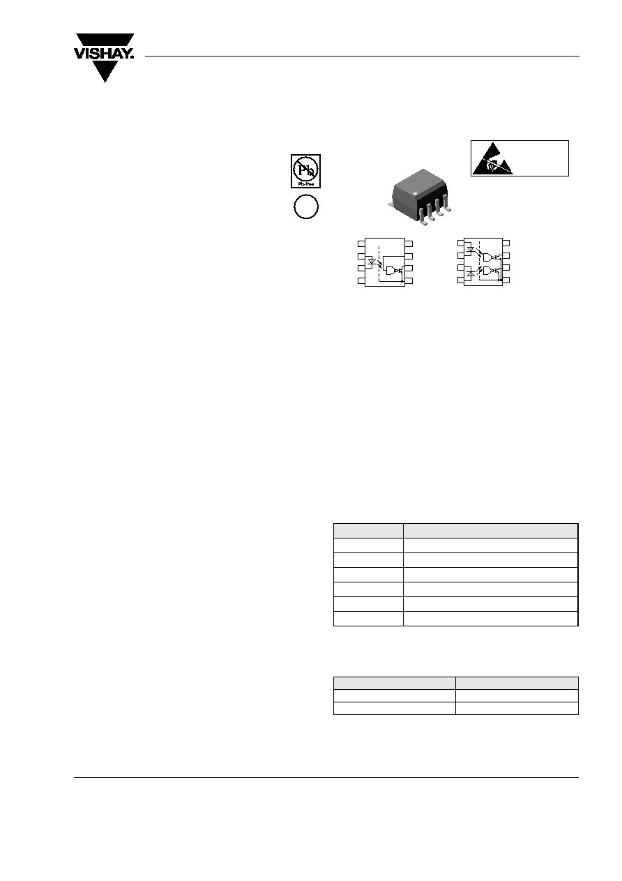
NC
A
C
NC
V CC
V E
V O
GND
A1
C1
C2
A2
V CC
V O1
V O2
GND
Single channel
Dual channel
VO0600T, VO0601T, VO0611T
18921-8
VO0630T, VO0631T, VO0661T
For Handing
Electrostatic Sensitive
Observe Precaution
ATTENTION
Devices (ESD)
20050
High Speed Optocoupler, 10 MBd
SOIC-8 Package
Features
∑ Choice of CMR performance of 10 kV/µs,
5 kV/µs, and 100 v/µs
∑ High speed: 10 MBd typical
∑ + 5 V CMOS compatibility
∑ Guaranteed AC and DC performance
over temperature: - 40 to + 100 ∞C Temp. Range
∑ Pure tin leads
∑ Meets IEC60068-2-42 (SO
2
) and
IEC60068-2-43 (H
2
S) requirements
∑ Low input current capability: 5 mA
∑ Lead (Pb)-free component
∑ Component in accordance to RoHS 2002/95/EC
and WEEE 2002/96/EC
Agency Approvals
∑ UL1577, File No. E52744
∑ CUL-File No. E52744, equivalent to CSA bulletin 5A
∑ DIN EN 60747-5-2 (VDE0884)
∑ Reinforced insulation rating per IEC 2.10.5.1
∑ VDE available with Option 1
Applications
∑ Microprocessor System Interface
∑ PLC, ATE input/output isolation
∑ Computer peripheral interface
∑ Digital Fieldbus Isolation: CC-Link, DeviceNet,
Profibus, SDS
∑ High speed A/D and D/A conversion
∑ AC Plasma Display Panel Level Shifting
∑ Multiplexed Data Transmission
∑ Digital control power supply
∑ Ground loop elimination
Description
The VO06xxT family are single and dual channel 10
MBd optocoupler utilizing a high efficient input LED
coupled with an integrated optical photodiode IC
detector. The detector has an open drain NMOS-tran-
sister output, providing less leakage compared to an
open collector Schottky clamped transister output.
For the single channel type, an enable function on
pin 7 allows the detector to be strobed. The internal
shield provides a guaranteed common mode tran-
sient immunity of 5 kV/µs for the VO0601T and
VO0631T and 10 kV/µs for the VO0611T and
VO0661T. The use of a 0.1 µF bypass capacitor con-
nected between pin 5 and 8 is recommended.
Order Information
Truth Table (Positive Logic)
Part
Remarks
VO0600T
100 V/µs, Single channel, SOIC-8
VO0601T
5 kV/µs, Single channel, SOIC-8
VO0611T
10 kV/µs, Single channel, SOIC-8
VO0630T
100 V/µs, Dual channel, SOIC-8
VO0631T
5 kV/µs, Dual channel, SOIC-8
VO0661T
10 kV/µs, Dual channel, SOIC-8
LED
OUTPUT
ON
L
OFF
H
e3
www.vishay.com
2
Document Number 84607
Rev. 1.4, 04-Jul-06
VO0600T/0601T/0611T/0630T/0631T/0661T
Vishay Semiconductors
Absolute Maximum Ratings
T
amb
= 25 ∞C, unless otherwise specified
Stresses in excess of the absolute Maximum Ratings can cause permanent damage to the device. Functional operation of the device is
not implied at these or any other conditions in excess of those given in the operational sections of this document. Exposure to absolute
Maximum Rating for extended periods of the time can adversely affect reliability.
Input
Output
Coupler
Recommended Operating Conditions
Parameter
Test condition
Symbol
Value
Unit
Average forward current (single channel)
I
F
15
mA
Average forward current (dual channel)
I
F
mA
Reverse input voltage
V
R
5
V
Enable input voltage (single channel)
V
E
V
CC
+ 0.5 V
V
Enable input current (single channel)
I
E
5
mA
Surge current
t = 100 µs
I
FSM
200
mA
Parameter
Test condition
Symbol
Value
Unit
Supply voltage
1 minute max.
V
CC
7
V
Output current
I
O
50
mA
Output voltage
V
O
7
V
Output power dissipation
(single channel)
P
diss
85
mW
Output power dissipation
(per channel for duals)
P
diss
60
mW
Parameter
Test condition
Symbol
Value
Unit
Storage temperature
T
stg
- 55 to + 150
∞C
Operating temperature
T
amb
- 40 to + 100
∞C
Lead solder temperature
for 10 sec.
260
∞C
Solder reflow temperature
for 1 minute
260
∞C
Isolation test voltage
t = 1.0 sec.
V
ISO
3000
V
RMS
Parameter
Test condition
Symbol
Min
Typ.
Max
Unit
Operating temperature
T
amb
- 40
100
∞C
Supply voltage
V
cc
4.5
5.5
V
Input current low level
I
FL
0
250
µA
Input current high level
I
FH
5
15
mA
Output pull up resistor
R
L
330
4 K
Logic high enable voltage
V
EH
2.0
V
CC
V
Logic low enable voltage
V
EL
0.0
0.8
V
Fanout
R
L
= 1 k
N
5
-
VO0600T/0601T/0611T/0630T/0631T/0661T
Document Number 84607
Rev. 1.4, 04-Jul-06
Vishay Semiconductors
www.vishay.com
3
Electrical Characteristics
T
amb
= 25 ∞C and V
cc
= 5.5 V, unless otherwise specified
Minimum and maximum values are testing requirements. Typical values are characteristics of the device and are the result of engineering
evaluation. Typical values are for information only and are not part of the testing requirements.
Input
Output
Switching Characteristics
Over Recommended Temperature (T
a
= - 40 to + 100 ∞C), V
CC
= 5 V, I
F
= 7.5 mA unless otherwise specified.
All Typicals at T
a
= 25 ∞C, V
CC
= 5 V.
Parameter
Test condition
Symbol
Min
Typ.
Max
Unit
Input forward voltage
I
F
= 10 mA
V
F
1.1
1.4
1.7
V
Reverse current
V
R
= 5.0 V
I
R
0.01
10
µA
Input capacitance
f = 1 MHz, V
F
= 0 V
C
I
55
pF
Parameter
Test condition
Symbol
Min
Typ.
Max
Unit
High level supply current
(single channel)
V
E
= 0.5 V, I
F
= 0 mA
I
CCH
4.1
7.0
mA
V
E
= V
CC
, I
F
= 0 mA
I
CCH
3.3
6.0
mA
High level supply current
(dual channel)
I
F
= 0 mA
I
CCH
6.5
12.0
mA
Low level supply current
(single channel)
V
E
= 0.5 V, I
F
= 10 mA
I
CCL
4.0
7.0
mA
V
E
= V
CC
, I
F
= 10 mA
I
CCL
3.3
6.0
mA
Low level supply current
(dual channel)
I
F
= 10 mA
I
CCL
6.5
12.0
mA
High level output current
V
E
= 2.0 V, V
O
= 5.5 V,
I
F
= 250 µA
I
OH
0.002
1
µA
Low level output voltage
V
E
= 2.0 V, I
F
= 5 mA,
I
OL
(sinking) = 13 mA
V
OL
0.2
0.6
V
Input threshold current
V
E
= 2.0 V, V
O
= 5.5 V,
I
OL
(sinking) = 13 mA
I
TH
2.4
5.0
mA
High level enable current
I
EH
- 0.6
- 1.6
mA
Low level enable current
I
EL
- 0.8
- 1.6
mA
High level enable voltage
V
EH
2.0
V
Low level enable voltage
V
EL
0.8
V
Parameter
Test condition
Symbol
Min
Typ.
Max
Unit
Propagation delay time to high
output level
R
L
= 350
, C
L
= 15 pF
t
PLH
20
48
100
ns
Propagation delay time to low
output level
R
L
= 350
, C
L
= 15 pF
t
PHL
25
50
100
ns
Pulse width distortion
R
L
= 350
, C
L
= 15 pF
| t
PHL
- t
PLH
|
2.9
35
ns
Propagation delay skew
R
L
= 350
, C
L
= 15 pF
t
PSK
8
40
ns
Output rise time (10 - 90 %)
R
L
= 350
, C
L
= 15 pF
t
r
23
ns
Output fall time (90 - 10 %)
R
L
= 350
, C
L
= 15 pF
t
f
7
ns
Propagation delay time of
enable from V
EH
to V
EL
R
L
= 350
, C
L
= 15 pF,
V
EL
= 0 V, V
EH
= 3 V
t
ELH
12
ns
Propagation delay time of
enable from V
EL
to V
EH
R
L
= 350
, C
L
= 15 pF,
V
EL
= 0 V, V
EH
= 3 V
t
EHL
11
ns
www.vishay.com
4
Document Number 84607
Rev. 1.4, 04-Jul-06
VO0600T/0601T/0611T/0630T/0631T/0661T
Vishay Semiconductors
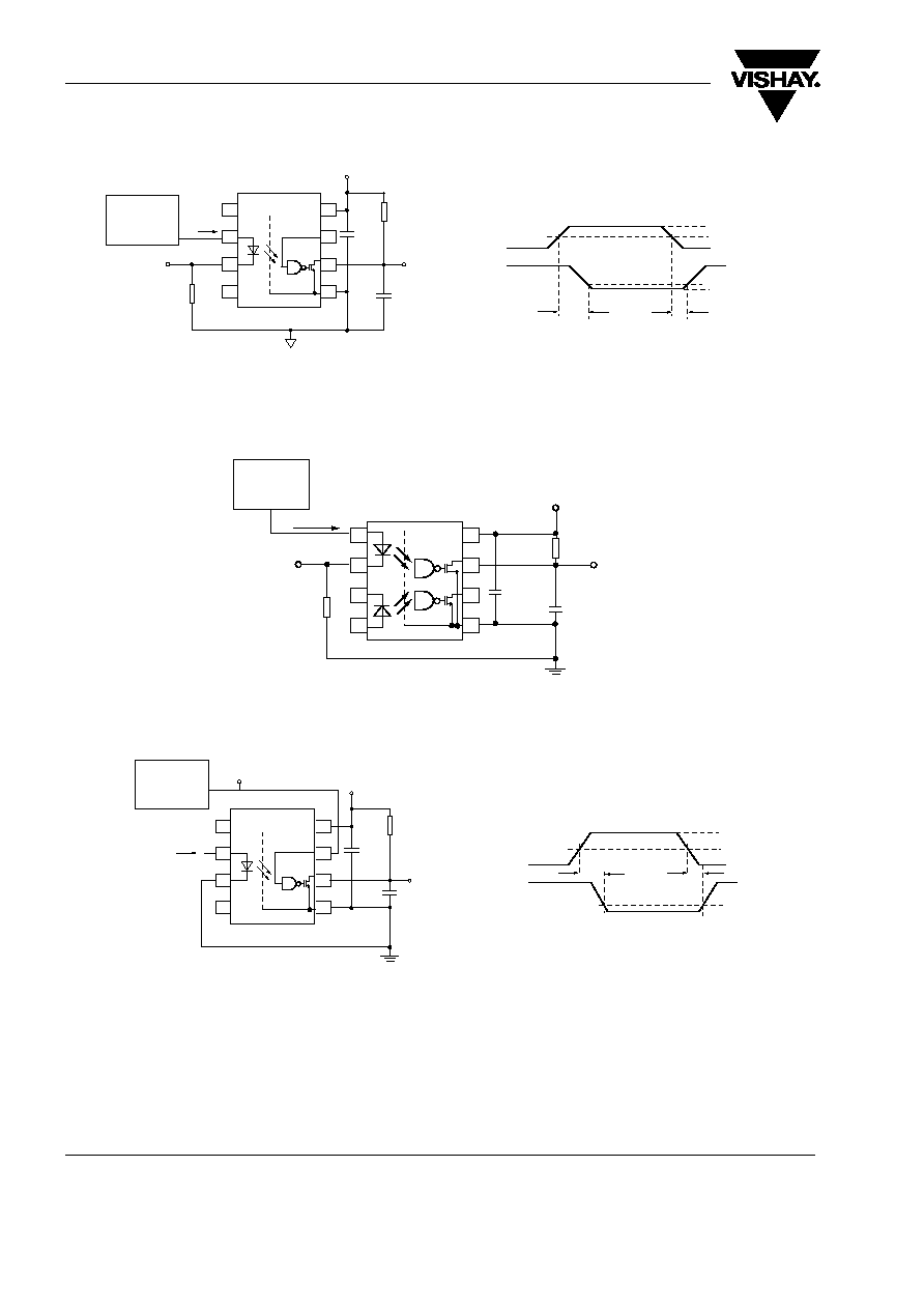
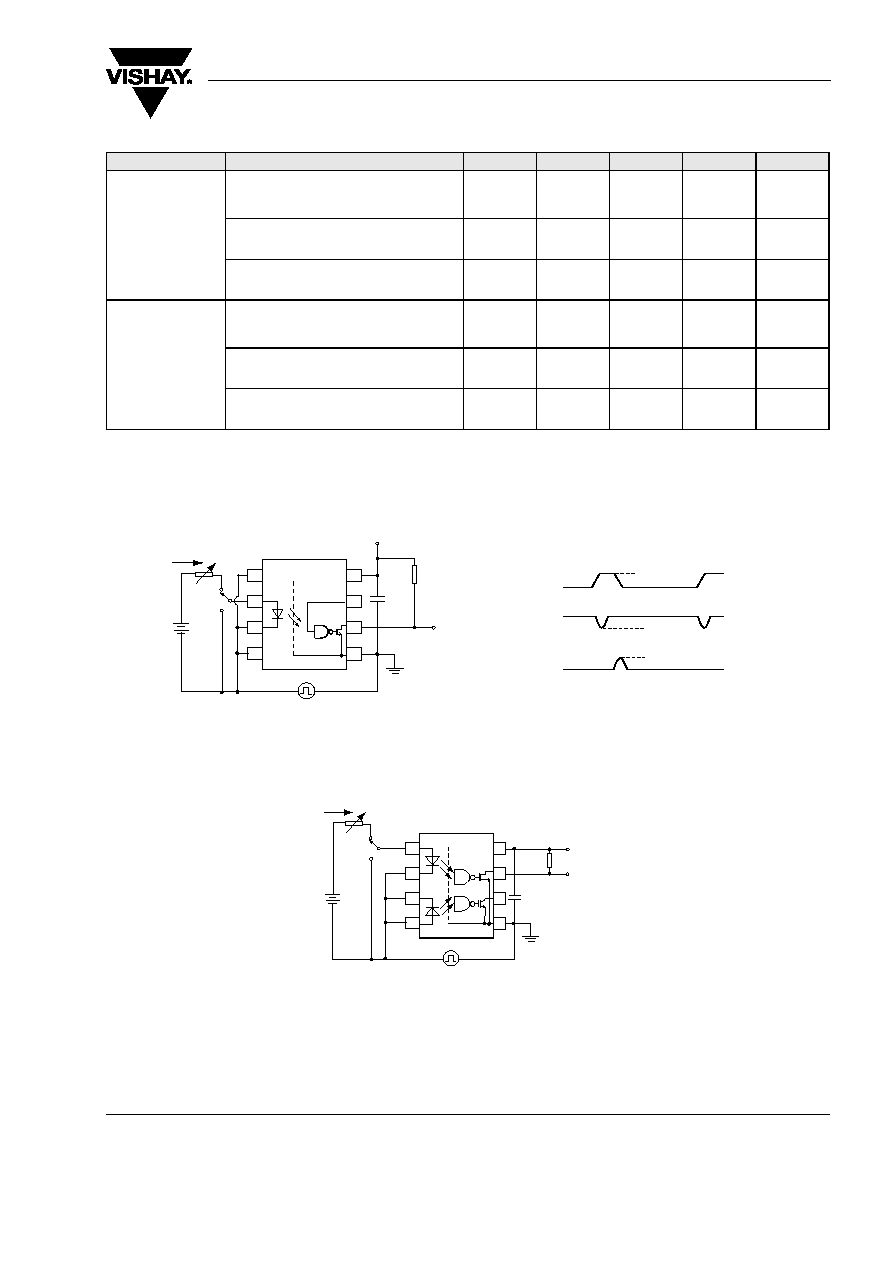
Figure 1. Single Channel Test Circuit for t
PLH
, t
PHL
, t
r
and t
f
Figure 2. Dual Channel Test Circuit for t
PLH
, t
PHL
, t
r
and t
f
Figure 3. Single Channel Test Circuit for t
EHL
, t
ELH
1
2
3
4
8
7
6
5
18964-2
The Probe and Jig Capacitances are included in C
Input I F
Output V O
I F
0 m A
V OL
1.5 V
t PHL
t PLH
V OH
C =
15 pF
GND
0. 1 µF
Bypass
VCC
VOUT
V CC
I F
R
R L
Inpu t I
F
Monitoring
Nod e
Output V O
Monitoring
Node
L
Single Channel
Pulse Gen.
Z =
50
t =
t = 5 n
s
o
f
r
M
L
= 7.5 mA
I F = 3.75 mA
V
E
1
2
3
4
Pulse Gen.
Z =
50
t =
t = 5 n
s
o
f
r
Input
Monitor ing
Node
Output V
Monitor ing
Node
O
I F
RM
R L
C L = 1 5 p F
0.1 µF
Bypass
18963-3
V CC
1
2
3
4
8
7
6
5
18975-2
The Probe and Jig Capacitances are included in C
Inpu t V
E
Output V O
t EH L
t ELH
C =
15 pF
GND
0.1 µF
Bypass
VCC
VOU T
V CC
I F
R L
Output V O
Monitoring
Node
L
Single Channel
Pulse Gen.
Z =
50
t =
t = 5 n
s
o
f
r
L
7.5 mA
Input V
Monitoring Node
E
3 V
1. 5 V
1. 5 V
VE
VO0600T/0601T/0611T/0630T/0631T/0661T
Document Number 84607
Rev. 1.4, 04-Jul-06
Vishay Semiconductors
www.vishay.com
5
Common Mode Transient Immunity
1)
For VO0600T and VO0630T
2)
For VO0601T and VO0631T
3)
For VO0611T and VO0661T
Parameter
Test condition
Symbol
Min
Typ.
Max
Unit
Common mode
transient immunity
(high)
|V
CM
| = 10 V, V
CC
= 5 V, I
F
= 0 mA,
V
O(min)
= 2 V, R
L
= 350
, T
amb
= 25 ∞C
1)
| CM
H
|
100
V/µs
|V
CM
| = 50 V, V
CC
= 5 V, I
F
= 0 mA,
V
O(min)
= 2 V, R
L
= 350
, T
amb
= 25 ∞C
2)
| CM
H
|
5000
10000
V/µs
|V
CM
| = 1 kV, V
CC
= 5 V, I
F
= 0 mA,
V
O(min)
= 2 V, R
L
= 350
, T
amb
= 25 ∞C
3)
| CM
H
|
10000
15000
V/µs
Common mode
transient immunity
(low)
|V
CM
| = 10 V, V
CC
= 5 V, I
F
= 7.5 mA,
V
O(max)
= 0.8 V, R
L
= 350
, T
amb
= 25 ∞C
1)
| CM
L
|
100
V/µs
|V
CM
| = 50 V, V
CC
= 5 V, I
F
= 7.5 mA,
V
O(max)
= 0.8 V, R
L
= 350
, T
amb
= 25 ∞C
2)
| CM
L
|
5000
10000
V/µs
|V
CM
| = 1 kV, V
CC
= 5 V, I
F
= 7 mA,
V
O(max)
= 0.8 V, R
L
= 350
, T
amb
= 25 ∞C
3)
| CM
L
|
10000
15000
V/µs
Figure 4. Single Channel Test Circuit for Common Mode Transient Immunity
Figure 5. Dual Channel Test Circuit for Common Mode Transient Immunity
VCM (PEAK)
Switch AT A: I 0 m
A
F
Switch AT A:
7. 5 m
A
F
V O (min.
V O (max.)
0 V
5 V
V
V
CM
V O
V
O 0. 5
CM H
CM L
1
2
3
4
8
7
6
5
18976-2
GND
0. 1
F
Bypass
V CC
VOUT
VCC
R L
Output V O
Monitoring
Node
+
-
VCM
Single Channel
B
A
V FF
I F
Pulse Generator
Z =
50
O
VE
)
=
I =
1
2
3
4
8
7
6
5
18977-1
GND
0. 1 µF
Bypass
VCC
R L
+ 5 V
Output V O
Monitoring
Node
+
-
V CM
B
A
V FF
I F
Pulse Generator
Z = 50
O
Dual Channel