For technical questions in the Americas, contact foilsupport1@vishay.com
For technical questions in Asia/Japan/Europe/Africa/Israel, contact foilsupport2@vishay.com
Document Number: 63061
Revision 17-Aug-04
www.vishay.com
22
VSM0805
Vishay Foil Resistors
SURF
ACE MOUNT
∑ ISRAEL: foilsales.israel@vishay.com ∑ FRANCE/SWITZERLAND/SOUTHERN EUROPE: foilsales.eusouth@vishay.com ∑ AMERICAS: foilsales.usa@vishay.com
∑ ASIA/JAPAN: foilsales.asia@vishay.com ∑ UK/HOLLAND/SCANDANAVIA: foilsales.eunorth@vishay.com ∑ GERMANY/CZECH REPUBLIC/AUSTRIA: foilsales.eucentral@vishay.com
SALES
Bulk Metal
Æ
Foil Technology
Discrete Surface Mount Chip Resistors
MIL-PRF-55342G
VSM
TEST
CHARACTERISTIC. E
MAXIMUM
R LIMITS
R LIMITS*
Thermal Shock
± 0.10%
± 0.02%
Low Temperature Operation
± 0.10%
± 0.02%
Short Time Overload
± 0.10%
± 0.02%
High Temperature Exposure
± 0.10%
± 0.05%
Resistance to Bonding
± 0.20%
± 0.05%
Moisture Resistance
± 0.20%
± 0.10%
Life 2000 hours @ + 70
∞
C
± 0.50%
± 0.025%
The VSM0805 represents the latest addition and smallest size
to the Precision Bulk Metal
Æ
Foil (BMF) technology surface
mount chip resistor series. The VSM0805 has a conventional
full wrap around termination.
The BMF technology offers designers the lowest and most
predictable absolute Temperature Coefficient Resistance
available. The TCR is a process capability not a selection
process and for the most part is independent of ohmic value
and lot related variations.
The availability of tight absolute tolerance provides a good cost
solution for the variability of other components when compiling
the total error budget. BMF offers the best stability available;
and is an order of magnitude better than thin film technology.
The noise generated by the resistor is non measurable and its
design and construction make it well suited for high frequency
applications. The BMF is the ultimate resistor component for
analog applications.
VALUE
TIGHTEST
(
)
TOLERANCE (%)*
250 to 12K
± 0.01
100 to < 250
± 0.02
50 to < 100
± 0.05
25 to < 50
± 0.1
10 to < 25
± 0.25
5.5 to <10
± 0.5
FEATURES
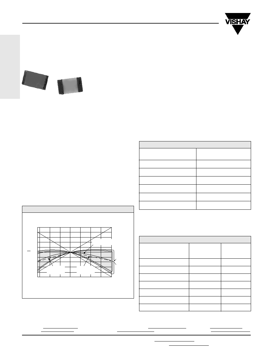
∑ Nominal TCR: + 0.6ppm/∞C (0 to 25∞C)
- 0.6ppm/C∞ (+ 25∞C to + 60∞C)
+ 2.2ppm/∞C (- 55∞C to + 25∞C)
- 1.8ppm/∞C (+ 25∞C to + 125∞C)
∑ Absolute Tolerance: to ± 0.01%
∑ Resistance Range: 5.5 to 12K
∑ Load Life Stability: ± 0.025% (2000 hours @ 70∞C)
∑ Shelf Life Stability: 0.005% Maximum R
∑ Voltage Coefficient: < 0.00001%/volt (< 0.1ppm/V)
∑ Current Noise: < - 40dB
∑ Non Inductive: < 0.08µH
∑ Terminal Finishes Available:
Lead (Pb)-free (Sn 99.3% Cu 0.7%)
Tin/Lead Alloy (Sn 62% Pb 36% Ag 2%)
*As shown + 0.01 Ohms to allow for measurement errors at low values.
The TCR for values < 100 are influenced by the termination
composition and result in a deviation from this curve. Contact our
application engineering department for detailed specification on low
values
TABLE 1 - TOLERANCE VERSUS RESISTANCE VALUE
*Tighter tolerances are available. Please contact Application
Engineering. Soldering temperatures used during installation may
cause resistance to shift up to 0.05%.
TABLE 2 - TYPICAL PERFORMANCE SPECIFICATIONS
FIGURE 1 - NOMINAL TCR CURVE
Product may not
be to scale
Maximum
Spread
±2.3 ppm/∞C
+125
≠55
≠50
≠25
0
+25
+50
+75
+100
+500
+400
+300
+200
+100
0
≠100
≠200
≠300
≠400
≠500
Standard
Spread
±2.0 ppm/∞C
+2.2 ppm/∞C
Nominal Chord
Slope (TCR)
≠1.8 ppm/∞C
Nominal Chord
Slope (TCR)
≠55∞C / +25∞C / +125∞C are the test points
with +25∞C as the reference temperature
R
R
(ppm)
Nominal Resistance/
Temperature (RT) Curve
+5 ppm
-5 ppm
For technical questions in the Americas, contact foilsupport1@vishay.com
For technical questions in Asia/Japan/Europe/Africa/Israel, contact foilsupport2@vishay.com
www.vishay.com
23
VSM0805
Vishay Foil Resistors
Document Number: 63061
Revision 17-Aug-04
SURF
ACE MOUNT
∑ ISRAEL: foilsales.israel@vishay.com ∑ FRANCE/SWITZERLAND/SOUTHERN EUROPE: foilsales.eusouth@vishay.com ∑ AMERICAS: foilsales.usa@vishay.com
∑ ASIA/JAPAN: foilsales.asia@vishay.com ∑ UK/HOLLAND/SCANDANAVIA: foilsales.eunorth@vishay.com ∑ GERMANY/CZECH REPUBLIC/AUSTRIA: foilsales.eucentral@vishay.com
SALES
Bulk Metal
Æ
Foil Technology
Discrete Surface Mount Chip Resistors
MODEL
CHIP SIZE
RESISTANCE VALUE
TOLERANCE TERMINATION
PACKAGING
VSM
0805
RESISTANCE
LETTER
MULTIPLIER
T ± 0.01%
S - Lead (Pb)-free
T = Tape and
RANGE
DESIGNATOR
FACTOR
Q ± 0.02%
B - Tin/Lead
Reel
A ± 0.05%
W = Waffle
5 to <1K
R
x 1.0
B ± 0.1%
PacK
Example: 249R00 = 249
C ± 0.25%
D ± 0.5%
F ± 1.0%
T
W
L
D
T
W
L
1K to 12K
K
x 10
3
Example: 10K000 = 10.0K
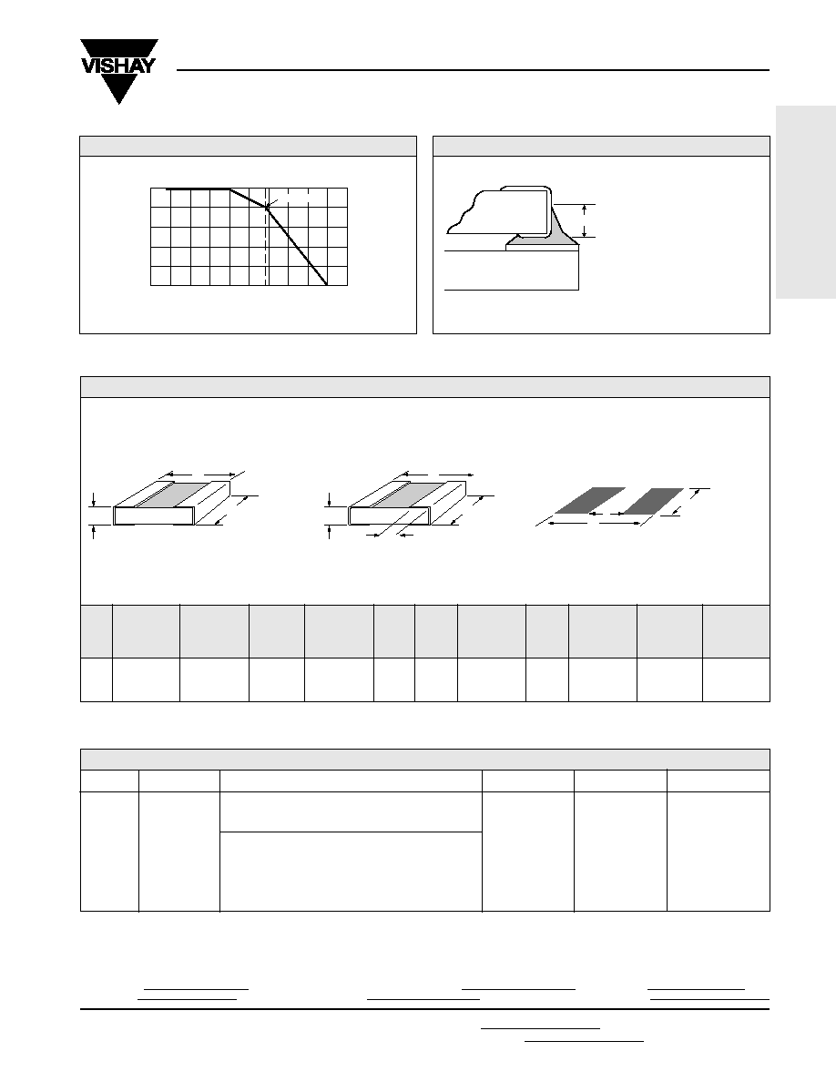
FIGURE 3 - RECOMMENDED MOUNTING
CHIP
POWER MAXIMUM RESISTANCE MAXIMUM
SIZE
L
W
T
D
+ 70
∞
C VOLTAGE
RANGE
WEIGHT
Z*
G*
X*
±
0.005 (0.13)
±
0.005 (0.13) MAXIMUM
±
0.005 (0.13) (mW)
(V)
(
)
(mG)
±
0.004 (0.10)
±
0.004 (0.10)
±
0.004 (0.10)
0805
0.080 (2.03)
0.050 (1.27) 0.025 (0.64) 0.015 (0.38)
50
22
5.5 - 12K
6
0.122 (3.10)
0.028 (0.70)
0.050 (1.27)
*Land Pattern Dimensions (Z, G, X) are per IPC-782A
TABLE 3 - CHIP SIZES AND SPECIFICATIONS in inches (millimeters)
TABLE 4 - ORDERING INFORMATION - VSM STYLE CHIP RESISTORS
FIGURE 2 - POWER DERATING CURVE
125
100
75
50
25
0
-75
≠50
≠25
0
+25
+50
+75
+100 +125 +150 +175
Ambient Temperature (∞C)
Percent of Rated Power
≠55∞C
+70∞C
Rated Power
Footprint
G
Z
X
Top View
Bottom View
Recommended Land Pattern
25% to 85% of T
A low profile solder fillet is recommended
to avoid unnecessary stresses along
top edge of metallization. IR and vapor
phase reflow are best. Avoid the use of
cleaning agents which could attack
epoxy resins, which form part of the
resistor construction.