 | –≠–ª–µ–∫—Ç—Ä–æ–Ω–Ω—ã–π –∫–æ–º–ø–æ–Ω–µ–Ω—Ç: VSC7809WC | –°–∫–∞—á–∞—Ç—å:  PDF PDF  ZIP ZIP |

VITESSE
SEMICONDUCTOR CORPORATION
Advance Product Information
VSC7809
Photodetector/Transimpedance Amplifier
Family for Optical Communication
G52195-0, Rev 2.4
Page 1
04/05/01
© VITESSE
SEMICONDUCTOR CORPORATION ∑ 741 Calle Plano ∑ Camarillo, CA 93012
Tel: (800) VITESSE ∑ FAX: (805) 987-5896 ∑ Email: prodinfo@vitesse.com
Internet: www.vitesse.com
Features
General Description
The VSC7809 integrated Photodetector/Transimpedance Amplifier provides a highly integrated solution
for converting light from a fiber optic communications channel into a differential output voltage. The benefits
of Vitesse Semiconductor's Gallium Arsenide H-GaAs process are fully utilized to provide very high bandwidth
and low noise in a product with a large optically active area for easy alignment. The sensitivity, duty cycle dis-
tortion and jitter meet or exceed all Fibre Channel and Gigabit Ethernet application requirements. Parts are
available in either die form, flat-windowed packages or in ball-lens packages.
By using a metal-semiconductor-metal (MSM) photodetector with a monolithic integrated transimpedance
amplifier, the input capacitance is lowered which allows for a larger optically active area than in discrete photo-
detectors. Integration also allows superior tracking over process, temperature and voltage between the photode-
tector and the amplifier, resulting in higher performance. This part can easily be used in developing Fibre
Channel Electro-Optic Receivers which exhibit very high performance and ease of use.
VSC7809 Block Diagram
Part Number
Data Rate
Bandwidth
(MHz)
Input Noise
(
µ
W rms)
Optically Active Area
(
µ
m diameter)
VSC7809
1.25Gb/s
800
1.4
100
∑ Integrated Photodetector/Transimpedance
Amplifier Optimized for High-Speed Optical
Communications Applications
∑ Fibre Channel/Gigabit Ethernet Compatible
∑ High Bandwidth
∑ Low Input Noise Equivalent Power
∑ Large Optically Active Area
∑ Single 3.3V Power Supply
Both DOUTP and DOUTN are back-terminated to 25
.
Photodetector/Transimpedance Amplifier
DOUTP
DOUTN
+3.3V
GND
VITESSE
SEMICONDUCTOR CORPORATION
Advance Product Information
VSC7809
Photodetector/Transimpedance Amplifier
Family for Optical Communication
Page 2
G52195-0, Rev 2.4
04/05/01
© VITESSE
SEMICONDUCTOR CORPORATION ∑ 741 Calle Plano ∑ Camarillo, CA 93012
Tel: (800) VITESSE ∑ FAX: (805) 987-5896 ∑ Email: prodinfo@vitesse.com
Internet: www.vitesse.com
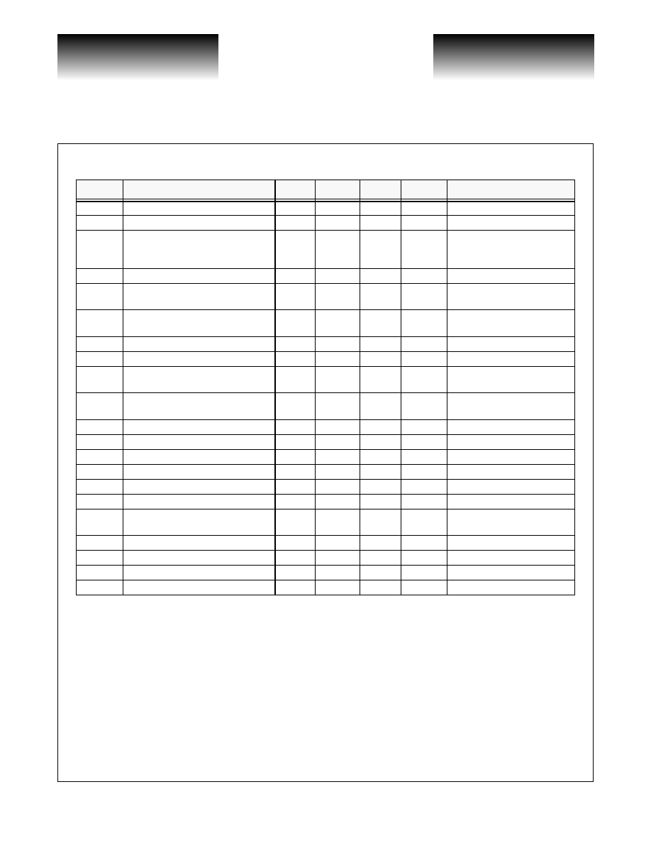
Table 1: Electro-Optical Specifications
(1)
Notes: (1) Specified over 0∞C (ambient) to 70∞C (case).
(2) Typical conditions 25∞C and 3.3V power supply.
(3) See Note 1 in Application Note 48.
(4) P = Incident Optical Power
(5) See Note 2 In Application Note 48.
Symbol
Parameter
Min
Typ
(2)
Max
Units
Conditions
V
SS
Supply Voltage
3.0
3.3
3.6
V
I
DD
Supply Current
14
23
40
mA
PSRR
Power Supply Rejection Ratio
-
-10
-
dB
Frequencies up to 40MHz
Use external filter to get
PSRR of -35dB
(3)
.
Wavelength
700
840
850
nm
f
C
Low Frequency Cutoff
-
1.8
2.5
MHz
-3db, P
(4)
= -15dBm @
50MHz
BW
Optical Modulation Bandwidth
800
1100
-
MHz
-3db,
P = -15dBm @ 50MHz
S
Sensitivity
-20
-21
dBm
1.25Gb/s, BER10
-12(5)
R
O
Single Ended Output Impedance
20
25
30
V
O
Differential Output Voltage
0.2
0.26
0.4
V
P = -5dBm,
R
LOAD
= 100
differential
R
D
Differential Responsivity
0.8
1.2
-
mV/
µ
W
R
LOAD
= 100
P = -15dBm @ 50MHz
V
DC
Output Bias Voltage
1.0
-
-
V
V
DC
Bias Offset Voltage
-
-
200
mV
NEP
O
Input Noise Equivalent Power
-
1
1.4
µ
W rms
P = 0mW
V
NO
Output Noise Voltage
-
1.0
1.25
mV rms
P = 0mW
DCD
Duty Cycle Distortion
-
-
4.5
%
P = -5dBm
I
OUT
Output Drive Current
2.0
2.6
-
mA
P = -5dBm
PDJ
Pattern Dependent Jitter
-
35
60
ps
P = -5dBm
+/-10% Voltage Window
----
Optically Active Area
-
100
-
µ
m Diameter
PPJ
PP Jitter
-
190
250
ps
P = -5 dBm
t
R
Rise Time
-
-
400
ps
20%-80% P = -5dBm
t
F
Fall Time
-
-
400
ps
20%-80% P = -5dBm

VITESSE
SEMICONDUCTOR CORPORATION
Advance Product Information
VSC7809
Photodetector/Transimpedance Amplifier
Family for Optical Communication
G52195-0, Rev 2.4
Page 3
04/05/01
© VITESSE
SEMICONDUCTOR CORPORATION ∑ 741 Calle Plano ∑ Camarillo, CA 93012
Tel: (800) VITESSE ∑ FAX: (805) 987-5896 ∑ Email: prodinfo@vitesse.com
Internet: www.vitesse.com
Table 2: Absolute Maximum Ratings
Table 3: Recommended Operating Conditions
Symbol
Parameter
Limits
V
SS
Power Supply
6V Required
T
STG
Storage Temperature
-55∞C to 125∞C (case temperature under bias)
H
STG
Storage Humidity
5 to 95% R.H. (including condensation)
H
OP
Operating Humidity
8 to 80% R.H. (excluding condensation)
P
INC
Incident Optical Power
+3dBm
IS Impact
Shock
500 G. Half Sine Wave
Pulse Duration 1 +/-0.5 ms
3 blows in each direction
V
IB
Vibration
20 > 2000 > 20Hz, 10 Minutes
10 G. Peak Acceleration
4 Complete Cycles, 3 Perpendicular Axes
Symbol
Parameter
Limits
V
SS
Power Supply
3.0VP-3.6V (3.3V nominal)
T
OP
Operating Temperature
0∞C (ambient) to 70∞C (case)
P
MAX
Maximum Optical Power
0dBm

VITESSE
SEMICONDUCTOR CORPORATION
Advance Product Information
VSC7809
Photodetector/Transimpedance Amplifier
Family for Optical Communication
Page 4
G52195-0, Rev 2.4
04/05/01
© VITESSE
SEMICONDUCTOR CORPORATION ∑ 741 Calle Plano ∑ Camarillo, CA 93012
Tel: (800) VITESSE ∑ FAX: (805) 987-5896 ∑ Email: prodinfo@vitesse.com
Internet: www.vitesse.com
Table 4: Pin Table Specifications for Ball Lens Packages, Flat Window Packages and Bare Die
NOTE: Pin Diagram is identical for both TO-46 and TO-56 package styles.
Figure 1: Pin Diagram
Figure 2: Schematic View of Bare Die Pad Assignments
Symbol
Description
DOUTP
Data output normal (with reference to incident light)
DOUTN
Data output complement (inverting) (with reference to incident light)
VSS
Power supply
GND
Ground (package case)
DOUTP
DOUTN
GND
VSS
Bottom View
DOUTN
GND
GND
GND
VSS
DOUTP

VITESSE
SEMICONDUCTOR CORPORATION
Advance Product Information
VSC7809
Photodetector/Transimpedance Amplifier
Family for Optical Communication
G52195-0, Rev 2.4
Page 5
04/05/01
© VITESSE
SEMICONDUCTOR CORPORATION ∑ 741 Calle Plano ∑ Camarillo, CA 93012
Tel: (800) VITESSE ∑ FAX: (805) 987-5896 ∑ Email: prodinfo@vitesse.com
Internet: www.vitesse.com
Package Information
(2x) 0.247
(2x) 0.1235
(2x) 0.18
1.04 ± 0.05
0.835
0.42
0.94
(4x) 0.055
(2x) 0.74
(2x) 0.29
0.35
(4x) 0.11
(2x) 0.15
1.68
1.48
1.58
0.05
DOUTN
GND
VSS
GND
DOUTP
GND
(4x) 0.365
(4x) 0.055
(6x) 0.11
0.05
0.1
VSC7809
0.05
0.05
Individual Die