 | –≠–ª–µ–∫—Ç—Ä–æ–Ω–Ω—ã–π –∫–æ–º–ø–æ–Ω–µ–Ω—Ç: VSC8021FC | –°–∫–∞—á–∞—Ç—å:  PDF PDF  ZIP ZIP |

VITESSE
SEMICONDUCTOR CORPORATION
G52028-0, Rev 4.1
Page 1
05/25/01
© VITESSE
SEMICONDUCTOR CORPORATION ∑ 741 Calle Plano ∑ Camarillo, CA 93012
Tel: (800) VITESSE ∑ FAX: (805) 987-5896 ∑ Email: prodinfo@vitesse.com
Internet: www.vitesse.com
Data Sheet
VSC8021/VSC8022
8-Bit MUX/DEMUX Chipset
2.5Gb/s SONET-Compatible
Features
Functional Description
The VSC8021 and VSC8022 are high-speed SONET interface devices capable of handling serial data at
rates up to 2.5Gb/s. These devices can be used for STS-3 through STS-48 SONET applications.
These products are fabricated in gallium arsenide using the Vitesse H-GaAs
E/D MESFET process which
achieves high-speed and low power dissipation. These products are packaged in a ceramic 52-pin leaded
ceramic chip carrier.
VSC8021
The VSC8021 contains an 8:1 multiplexer and a self-positioning timer. The 8:1 multiplexer accepts 8 paral-
lel differential ECL data inputs (D1-D8, D1N-D8N) at rates up to 312.5Mb/s and multiplexes them into a serial
differential bit stream output (DO, DON) at rates up to 2.5Gb/s.
The internal timing of the VSC8021 is built around the high-speed clock (up to 2.5GHz) delivered onto the
chip through a differential input (CLKI, CLKIN). This signal is subsequently echoed at the high-speed differen-
tial output (CO, CON).
The parallel data inputs are clocked to on-chip input registers with an externally supplied differential ECL
input (BYCLK, BYCLKN) operating at the same rate as the data inputs. An internal byte clock, which is a
divide-by-8 version of the high-speed clock, is used to transfer the data to a set of buffer registers. This internal
byte clock is brought off chip at the ECL output CLK8, CLK8N.
Internal circuitry monitors the internal and external byte clocks and generates an ERR signal if a timing
violation is detected. This signal can be gated to the SYNC input which is edge sensitive high. An active SYNC
input allows the VSC8021 timing to shift, positioning it properly against the external byte clock, CLK8,
CLK8N. When a CLK8 timing switch is made, normal data flow will be invalid for 1 byte.
There are two clock inputs, CLKI and BYCLK, going into the VSC8021. These two clocks serve as timing
references for different parts of the VSC8021. The BYCLK is used to trigger the input registers for the parallel
data inputs, while the CLKI is used to trigger the high-speed serial output register as well as some of the timing
circuitry for the parallel to serial conversion. Furthermore, in order to make this part easy to use, the user is not
required to assume a known phase relationship between CLKI and the BYCLK.
∑ Differential or Single-Ended Inputs and Outputs
∑ Low Power Dissipation: 2.3W (Typ Per Chip)
∑ Standard ECL Power Supplies:
V
EE
= -5.2V, V
TT
= -2.0V
∑ Available in Commercial (0
∞
C to +70
∞
C) or Industrial
(-40
∞
C to +85
∞
C) Temperature Ranges
∑ Proven E/D Mode GaAs Technology
∑ 52-Pin Leaded Ceramic Chip Carrier
∑ Serial Data Rates up to 2.5Gb/s
∑ Parallel Data Rates up to 312.5Mb/s
∑ ECL 100K Compatible Parallel Data I/Os
∑ Divide-by-8 Clock for Synchronization of
Parallel Data to Interfacing Chips
∑ SONET Frame Recovery Circuitry
(VSC8022)
∑ Compatible with STS-3 to STS-48
SONET Applications

VITESSE
SEMICONDUCTOR CORPORATION
Data Sheet
VSC8021/VSC8022
2.5Gb/s SONET-Compatible
8-Bit MUX/DEMUX Chipset
Page 2
G52028-0, Rev 4.1
05/25/01
© VITESSE
SEMICONDUCTOR CORPORATION ∑ 741 Calle Plano ∑ Camarillo, CA 93012
Tel: (800) VITESSE ∑ FAX: (805) 987-5896 ∑ Email: prodinfo@vitesse.com
Internet: www.vitesse.com
An internal Phase Detector and Phase Adjust Circuit are used to facilitate the two asynchronous circuits to
work with each other. The Phase Detector and the Phase Adjust Circuit work together to adjust the internal
clock CLK8 to make sure the set up and hold conditions are met for the internal registers. CLK8 is derived from
CLKI and the RCLK is a non-phase varying byte clock output. The edge sensitive SYNC signal is simply the
control signal that enables the Phase Detector circuitry.
As a summary, the CLKI is the high-speed clock input. The BYCLK is the external byte clock. The CLK8
is the internal byte clock derived from CLKI, phase-adjusted if SYNC is enabled. The RCLK is a non-phase-
adjusted divided-by-8 clock generated from CLKI. The phase of RCLK, RCLKN is not affected by the self-
adjusting circuitry, therefore it can be used as a system reference clock. RCLK, RCLKN can be used by the sys-
tem designer to generate BYCLK, BYCLKN. The self-positioning timer and RCLK, RCLKN allow for the cre-
ation of very tight parallel data timing for the VSC8021.
Figure 1: VSC8021 Block Diagram
ERR
Phase Adjustable
Byte Clock Output
CLK8
CLK8N
Serial Data Output
8:1
Multiplexer
Timing
Generator
DO
DON
High Speed
Clock Inputs
CLKI
CLKIN
Byte Clock
Inputs
BYCLK
BYCLKN
High Speed
Clock
CO
CON
Independent
Byte Clock Output
RCLK
RCLKN
8
8
Parallel
Data
D1
D1N
D8
D8N
Phase
Adjust
SYNC

VITESSE
SEMICONDUCTOR CORPORATION
G52028-0, Rev 4.1
Page 3
05/25/01
© VITESSE
SEMICONDUCTOR CORPORATION ∑ 741 Calle Plano ∑ Camarillo, CA 93012
Tel: (800) VITESSE ∑ FAX: (805) 987-5896 ∑ Email: prodinfo@vitesse.com
Internet: www.vitesse.com
Data Sheet
VSC8021/VSC8022
8-Bit MUX/DEMUX Chipset
2.5Gb/s SONET-Compatible
VSC8022
The VSC8022 contains both a 1:8 demultiplexer and SONET frame recovery circuitry. The 1:8 demultiplexer
accepts a serial data input (
DI, DIN
) at rates up to 2.5Gb/s and converts it into 8 parallel differential ECL data outputs
(
D1-D8, D1N-D8N
) at rates up to 312.5Mb/s. Valid parallel data outputs are indicated by the divide by 8 differential
clock outputs
BYCKO, BYCKON
.
The VSC8022 also contains a SONET frame recovery circuit. The frame recovery circuits are enabled by a fall-
ing edge on the
OOFN
ECL input when the
FDIS
input is low. Once enabled, the frame recovery circuit starts look-
ing for the SONET framing sequence. Once the frame is detected, the word boundary is realigned, a confirmation
signal is sent off-chip through the
FP
ECL output and the frame recovery circuits are disabled. While the frame
aligner is hunting for the frame,
BYCKO, BYCKON
and parallel data are invalid.
Figure 2: VSC8022 Block Diagram
Frame recovery circuits are disabled by frame detection (resulting in FP) or by a falling edge on the OOFN
input while FDIS is high.
Parallel
Data Outputs
Serial Data In
1:8
Demultiplexer
Timing
Generator
High Speed
Clock Inputs
-- Frame Detection Signal
DI
D1
CLKI
CLKIN
DIN
D1N
Byte Clock Out
BYCKO
BYCKON
FP
D8
D8N
SONET
Frame
Detection &
Recovery
FDIS
OOFN
Frame Recovery Disable --
Frame Recovery Clock --

VITESSE
SEMICONDUCTOR CORPORATION
Data Sheet
VSC8021/VSC8022
2.5Gb/s SONET-Compatible
8-Bit MUX/DEMUX Chipset
Page 4
G52028-0, Rev 4.1
05/25/01
© VITESSE
SEMICONDUCTOR CORPORATION ∑ 741 Calle Plano ∑ Camarillo, CA 93012
Tel: (800) VITESSE ∑ FAX: (805) 987-5896 ∑ Email: prodinfo@vitesse.com
Internet: www.vitesse.com
VSC8021 Multiplexer AC Characteristics
(Over recommended operating conditions)
Figure 3: VSC8021 Multiplexer Waveforms
Table 1: VSC8021 Multiplexer AC Characteristics
(over recommended operating conditions)
NOTES: (1) The parts are guaranteed by design to operate from DC to a maximum frequency of 2.5GHz.
(2) Required when SYNC not connected to ERR.
Parameter
Description
Min
Typ
Max
Units
Conditions
t
C
Clock period
(1)
400
ps
t
D
BYTE clock period (t
D
= t
C
x 8)
3.2
ns
t
DSU
Parallel data set-up time
0.6
ns
t
DH
Data hold time
1.4
ns
t
CMD
High-speed clock output (CO, CON) timing, falling
edge of CO to muxed data output, (DO, DON) timing
220
350
ps
t
BCLK8
Byte clock to CLK8 timing
(2)
0.5
1.0
1.5
ns
Jitter (p-p)
CLKI, CLKIN to DO, DON (max-min), (HI to LO),
same part, same pin at constant conditions
<50
ps
t
D
t
C
VALID DATA(2)
t
DH
Serialized Byte 1
D01
D02
D03
D04
D05
D06
D07
D08
t
DSU
VALID DATA(1)
t
CMD
NOTES:
= Don't care.
period x 8 =
period.
CLKI (CLKIN)
BYCLK (BYCLKN)
(1) Negative edge is active edge.
(2) BYCLK/CLK8 timing required when SYNC not connected to ERR.
tBCLK8
High speed differential clock input
D1-D8, D1N-D8N
CO, CON
DO,DON
Byte clock input
Parallel differential data inputs
High speed differential clock outputs
High speed differential data outputs
SYNC
CLK8 adjustment input
CLKI , CLKIN
(1)
BYCLK (BYCLKN)
(1)
Phase adjustable ˜8 output
CLK8
(2)
VITESSE
SEM
I
C
ONDUCT
OR CO
RP
O
R
A
T
I
O
N
G52
028
-0
, Re
v 4.1
Page 5
05/
25/0
1
©
VI
TES
S
E
SEM
ICONDUCT
OR CO
RPORAT
I
O
N
∑
7
41
C
a
l
l
e
P
l
a
no
∑
Ca
m
a
r
illo
,
CA 9
3
0
1
2
T
e
l:
(
8
0
0
)
VI
TES
SE
∑
F
A
X
:
(8
05)
98
7-
589
6
∑
Em
a
il: p
r
o
d
in
fo
@vite
s
s
e
.co
m
In
te
r
n
e
t
: www.vit
e
sse
.co
m
Da
t
a
S
h
e
e
t
VSC
802
1/VSC80
22
8-
Bi
t MU
X/
DE
MUX
Chi
p
s
e
t
2.5
G
b/s SONET
-
Co
mp
atib
le
VS
C
8
022 A
C
Ch
a
r
ac
ter
i
sti
cs
(O
ve
r rec
o
m
m
e
n
d
ed o
per
atin
g c
o
n
d
it
ion
s
)
F
i
g
u
r
e 4
:
VS
C802
2 De
mu
lt
ip
lexe
r W
ave
f
o
r
m
s
A1
A1
D1 (D1N)
D2 (D2N)
D3 (D3N)
D4 (D4N)
D5 (D5N)
D6 (D6N)
D7 (D7N)
D8 (D8N)
t
PFP
A2
A2
A2
Data
Data
Data
Data
Valid
Data
Valid
Data
Valid
Data
Valid
Data
Valid
Data
Valid
Data
Valid
Data
Valid
Data
Valid
Data
Valid
Data
Valid
Data
Valid
Data
Valid
Data
Valid
Data
Valid
Data
Valid
Data
FP
Parallel Data∑
Output Summary
t
DFP
t
C
A1
A1
A1
A2
A2
A2
DATA
t
OOFN
t
OOFNPW
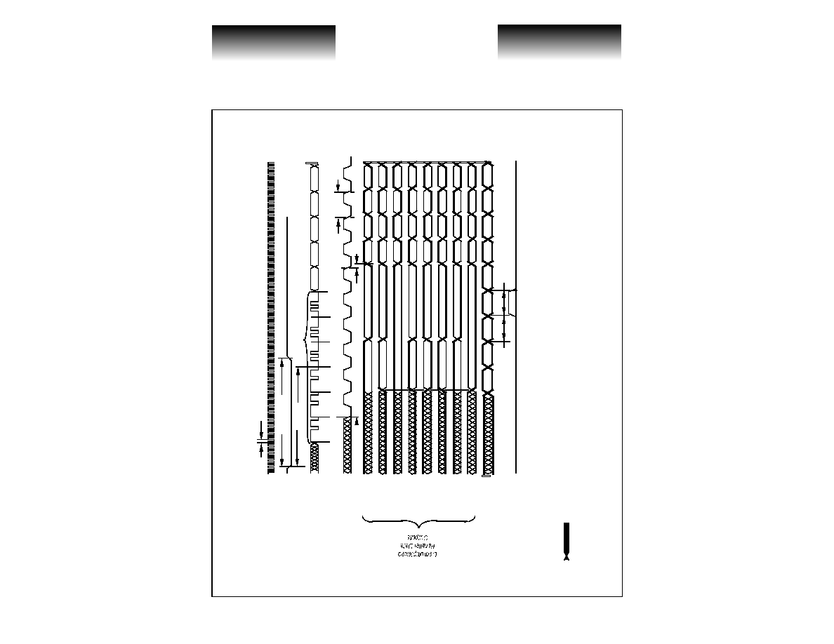
SONET STS-3 Framing Sequence
DATA
DATA
DATA
DATA
t
BD
Resynch
BYCKO
t
D
CLKI (CLKIN)
OOFN
DI (DIN)
BYCKO (BYCKON)
High speed differential clock input
Frame recovery clock input
High speed serial data inputs
Frame detection confirm output
Byte clock output
(1)
1) Negative edge is active edge.
2) The parallel data outputs only begin showing valid data after the last A2 of the SONET framing sequence. The example
waveforms shown above use an STS-3 framing sequence for convenience, thus valid data is output after the third
A2 in the sequence.
= Don't care.
NOTES:
(2)