 | –≠–ª–µ–∫—Ç—Ä–æ–Ω–Ω—ã–π –∫–æ–º–ø–æ–Ω–µ–Ω—Ç: VSC8061FI | –°–∫–∞—á–∞—Ç—å:  PDF PDF  ZIP ZIP |
VITESSE
SEMICONDUCTOR CORPORATION
G52069-0, Rev 4.3
Page 1
05/11/01
©
VITESSE
SEMICONDUCTOR CORPORATION ∑ 741 Calle Plano ∑ Camarillo, CA 93012
Tel: (800) VITESSE ∑ FAX: (805) 987-5896 ∑ Email: prodinfo@vitesse.com
Internet: www.vitesse.com
Data Sheet
VSC8061/VSC8062
Multiplexer/Demultiplexer Chipset
2.5Gb/s 16-Bit
Features
Functional Description
The VSC8061 and VSC8062 are high-speed interface devices capable of data rates up to 2.5Gb/s. The
devices are fabricated in gallium arsenide using the Vitesse H-GaAs E/D MESFET process to achieve high-
speed and low power dissipation. For ease of system design using these products, both devices use industry-
standard -5.2V and -2V power supplies, and have ECL-compatible I/O for parallel data interfaces. Typical
applications include telecommunication transmission and instrumentation.
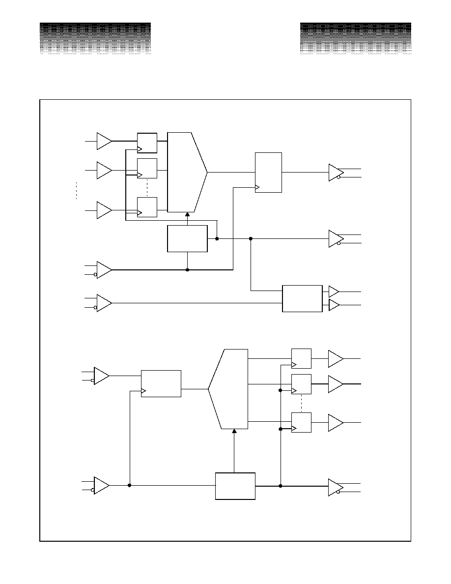
VSC8061 Multiplexer
The VSC8061 consists of a 16:1 multiplexer circuit, a phase detector, and a timing circuit which generates
a divide-by-16 clock from the high-speed clock input. The 16:1 multiplexer accepts 16 parallel single-ended
ECL compatible inputs (D0...D15) at data rates up to 156Mb/s and bitwise serializes them into a 2.5Gb/s serial
output (DO/DON). The internal timing of the VSC8061 is referenced to the negative going edge of the high-
speed clock true input (CLK). This clock is divided by 16 and is provided as an output (CLK16/CLK16N). The
setup and hold time of the parallel inputs (D[0:15]) are specified with respect to the falling edge of CLK16, so
that CLK16/CLK16N can be used to clock the data source of D[0:15]. The on-chip phase detector monitors the
phase relationship between the internally generated divide-by-16 clock and an externally supplied low-speed
reference clock input (DCLK/DCLKN). Phase difference between these two clock signals generates an up or
down output (U, D) for phase lock applications. The phase detector can be used as part of an external Phase
Locked Loop (PLL) to implement a clock multiplication function.
In applications where a 2.5GHz system clock is provided, and the phase detector function is not required, it
is recommended to connect one side of the DCLK/DCLKN input to V
TT
through a 50
resistor. The U and D
output can be left open and unused.
VSC8062 Demultiplexer
The VSC8062 consists of a 1:16 demultiplexer and timing circuitry which generates a divide-by-16 clock
from the high-speed clock input. The demultiplexer accepts a serial data stream input (DI/DIN) at up to 2.5Gb/s
and deserializes it into 16 parallel single-ended ECL compatible outputs (D[0:15]) at data rates up to 156 Mb/s.
The internal timing of the VSC8062 is referenced to the negative going edge of the high-speed clock true input
(CLK). This clock is divided by 16 and provided as an output (CLK16/ CLK16N). The timing parameters of the
parallel data outputs (D[0:15]) are specified with respect to the falling edge of CLK16, so that CLK16/CLK16N
can be used to clock the destination of D[0:15].
∑ Serial Data Rate up to 2.5Gb/s
∑ 16-Bit Wide ECL 100K Compatible Parallel Data
Interface
∑ Differential High-Speed Data Outputs
∑ Differential or Single-Ended High-Speed Data and
Clock Inputs
∑ On-Chip Phase Detector (VSC8061 Multiplexer)
∑ Power Dissipation: VSC8061:2.0W(max),
VSC8062: 1.7W(max)
∑ Standard ECL Power Supplies: V
EE
= -5.2V,
V
TT
= -2.0V
∑ Commercial (0
o
C to +70
o
C) or Industrial (-40
o
C
to +85
o
C) Temperature Range
∑ Available in 52-Pin Ceramic Leaded Chip Carrier
or 52-Pin Plastic Quad Flat Pack Packages
VITESSE
SEMICONDUCTOR CORPORATION
Data Sheet
VSC8061/VSC8062
2.5Gb/s 16-Bit
Multiplexer/Demultiplexer Chipset
Page 2
G52069-0, Rev 4.3
05/11/01
©
VITESSE
SEMICONDUCTOR CORPORATION ∑ 741 Calle Plano ∑ Camarillo, CA 93012
Tel: (800) VITESSE ∑ FAX: (805) 987-5896 ∑ Email: prodinfo@vitesse.com
Internet: www.vitesse.com
Figure 1: VSC8061 Block Diagram
Figure 2: VSC8062 Block Diagram
16:1
Multiplexer
Output
Register
Timing
Generator
Phase
Detector
D
0
D
1
D
15
CLK
CLKN
DCLK
DCLKN
DO
DON
CLK16
CLK16N
U
D
Bit Rate Clock
Parallel Data
Receivers
Input
Registers
Timing
Generator
CLK16
CLK16N
CLK
CLKN
DI
DIN
Input
Register
1:16
De-
Multiplexer
D
0
D
1
D
15
Parallel Data
Outputs
Output
Registers
VITESSE
SEMICONDUCTOR CORPORATION
G52069-0, Rev 4.3
Page 3
05/11/01
©
VITESSE
SEMICONDUCTOR CORPORATION ∑ 741 Calle Plano ∑ Camarillo, CA 93012
Tel: (800) VITESSE ∑ FAX: (805) 987-5896 ∑ Email: prodinfo@vitesse.com
Internet: www.vitesse.com
Data Sheet
VSC8061/VSC8062
Multiplexer/Demultiplexer Chipset
2.5Gb/s 16-Bit
VSC8061 Multiplexer AC Characteristics
(Over recommended operating range)
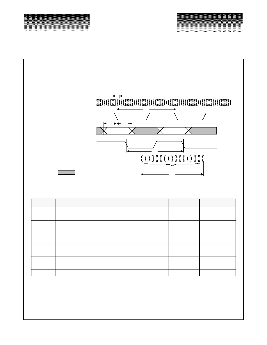
Figure 3: VSC8061 Multiplexer Waveforms
Table 1: VSC8061 AC Characteristics
NOTE: (1) Devices are guaranteed to operate to a maximum frequency of 2.5GHz.
Parameter
Description
Min
Typ
Max
Units
Conditions
t
CLK
Clock period
(1)
400
ps
t
D
CLK16, DCLK period (t
CLK
x 16)
6.4
15.6
ns
t
DSU
Parallel data set-up time with respect to CLK16
falling edge
2.0
ns
t
DH
Data hold time with respect to CLK16 falling
edge
0.5
ns
t
DC
CLK16 duty cycle
40
60
%
t
R
, t
F
DCLK (DCLKN) rise and fall times
1.5
ns
10% to 90%
t
R
, t
F
D[0:15] rise and fall times
2.0
ns
10% to 90%
t
R
, t
F
CLK16 (CLK16N) rise and fall times
0.5
1.0
ns
10% to 90%
t
R
, t
F
DO (DON) rise and fall times
150
165
ps
20% to 80%
VALID DATA (1)
VALID DATA (2)
D0 D1 D2 D3 D4 D5 D6 D7 D8 D9 D10 D11 D12 D13 D14 D15
High-speed differential clock input
Parallel data clock output
Parallel data inputs
Parallel data clock input
High-speed differential serial data output
CLK (CLKN)
CLK16 (CLK16N)
D[0:15]
DCLK (DCLKN)
DO (DON)
Serialized Data
t
D
t
D
t
D
t
DH
t
DSU
t
CLK
NOTE:
=
Don't care

VITESSE
SEMICONDUCTOR CORPORATION
Data Sheet
VSC8061/VSC8062
2.5Gb/s 16-Bit
Multiplexer/Demultiplexer Chipset
Page 4
G52069-0, Rev 4.3
05/11/01
©
VITESSE
SEMICONDUCTOR CORPORATION ∑ 741 Calle Plano ∑ Camarillo, CA 93012
Tel: (800) VITESSE ∑ FAX: (805) 987-5896 ∑ Email: prodinfo@vitesse.com
Internet: www.vitesse.com
VSC8061 Phase Detector Logic Diagram
The internal phase detector of the VSC8061 compares the phase difference between the internally gener-
ated divide-by-16 clock and the DCLK input. If both inputs (CLK16 and DCLK) to the phase detector are in
phase, the U and D outputs will both be low. If the rising edge of CLK16 precedes DCLK, a series of pulses
with pulse widths proportional to the phase difference will be present at the U output. Conversely, if DCLK pre-
cedes CLK16, then a series of pulses with widths proportional to the phase difference will be present at the D
output. The other output will remain low. The Phase Detector ignores phase differences for falling edges. This
circuitry is useful for implementing a Clock Multiplier Unit (CMU) function with the VSC8061. For example,
the DLCK can be the system reference clock at the parallel data rate. An external Voltage Controlled Oscillator
(VCO) at 16x the frequency of the reference clock can be used as the CLK input for the VSC8061. The phase
detector outputs (U and D) can then be used by an external integrator to generate an output that controls the
VCO. The generated 16x clock from the VCO will be phase-locked to the reference clock.
Figure 4: VSC8061 Phase Detector Logic Diagram
Figure 5: Phase Detector Input and Output Waveforms
CLK16
R
S
Q
S
R Q
U
D
DCLK
CLK16
DCLK
U
D
~ ~
~ ~
~ ~
~ ~

VITESSE
SEMICONDUCTOR CORPORATION
G52069-0, Rev 4.3
Page 5
05/11/01
©
VITESSE
SEMICONDUCTOR CORPORATION ∑ 741 Calle Plano ∑ Camarillo, CA 93012
Tel: (800) VITESSE ∑ FAX: (805) 987-5896 ∑ Email: prodinfo@vitesse.com
Internet: www.vitesse.com
Data Sheet
VSC8061/VSC8062
Multiplexer/Demultiplexer Chipset
2.5Gb/s 16-Bit
VSC8062 Demultiplexer AC Characteristics
(Over recommended operating range)
Figure 6:
VSC8062 Timing Diagram
Table 2: VSC8062 AC Characteristics
NOTES: (1) If t
CLK
changes, all remaining parameters change as indicated by the equations.
(2) t
SU
and t
H
are setup and hold times of the serial data input register.
(3) At t
CLK
= 400ps.
Parameter
Description
Min
Typ
Max
Units
Conditions
t
CLK
Clock period
(1)
400
ps
t
D
BYTE CLK16 period (t
CLK
x 16)
6.4
ns
t
DSU
CLK16 falling edge output to valid data
1.0
3.0
ns
t
DH
Phase Margin
=
Serial data phase timing margin with respect to
high-speed clock
(2)
180
(3)
degrees
t
CLK
High-speed differential clock input
CLK (CLKN)
High-speed serial data input
DI (DIN)
Parallel data clock output
CLK16
D0
D1
D15
t
D
t
BD
D
e
m
u
l
t
i
p
l
e
x
e
d
P
a
r
a
l
l
e
l
D
a
t
a
O
u
t
p
u
t
s
t
D
1
t
SU
t
H
+
t
CLK
-------------------
≠
360
∞
◊