
G52154-0, Rev 4.2
©
VITESSE
SEMICONDUCTOR CORPORATION
Page 1
3/19/99
741 Calle Plano, Camarillo, CA 93012 ∑ 805/388-3700 ∑ FAX: 805/987-5896
VITESSE
SEMICONDUCTOR CORPORATION
Data Sheet
VSC8113
ATM/SONET/SDH 622 Mb/s Transceiver Mux/Demux
with Integrated Clock Generation and Clock Recovery
Features
General Description
The VSC8113 is an ATM/SONET/SDH compatible transceiver integrating an on-chip Clock Multiplication
Unit (PLL) for the high speed clock as well as a clock and data recovery unit (CRU) with 8 bit serial-to-parallel
and parallel-to-serial data conversion. The PLL clock is used for serialization in the transmit direction (Mux).
The recovered clock is used for deserialization in the receive direction (Demux). The demultiplexer contains
SONET/SDH frame detection and recovery. The device provides both facility and equipment loopback modes
and two loop timing modes. The part is packaged in a 100PQFP with integrated heat spreader for optimum ther-
mal performance and reduced cost. The VSC8113 provides an integrated solution for ATM physical layers and
SONET/SDH systems applications.
Functional Description
The VSC8113 is designed to provide a SONET/SDH compliant interface between the high speed optical
networks and the lower speed User Network Interface devices such as the PM5355 S/UNI-622. The VSC8113
converts 8 bit parallel data at 77.76Mb/s or 19Mb/s to a serial bit stream at 622.08Mb/s or 155.52Mb/s respec-
tively. The device also provides a Facility Loopback function which loops the received high speed data and
clock (optionally recovered on-chip) directly to the high speed transmit outputs. A Clock Multiplier Unit
(CMU) is integrated into the transmit circuit to generate the high speed clock for the serial output data stream
from input reference frequencies of 19.44, 38.88, 51.84 or 77.76 MHz. The CMU can be bypassed with the
received/recovered clock in loop timing mode thus synchronizing the entire part to a single clock. The block
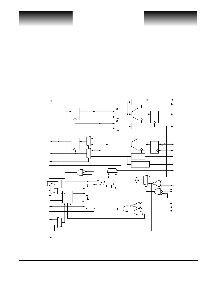
diagram on page 2 shows the major functional blocks associated with the VSC8113.
The receive section provides the serial-to-parallel conversion, converting the 155.52Mb/s or 622Mb/s bit
stream to an 8 bit parallel output at 19.44Mb/s or 77.76MHz respectively. A Clock Recovery Unit (CRU) is inte-
grated into the receive circuit to recover the high speed clock from the received serial data stream. The receive
section provides an Equipment Loopback function which will loop the low speed transmit data and clock back
through the receive section to the 8 bit parallel data bus and clock outputs.The VSC8113 also provides the
option of selecting between either its internal CRU's recovered clock and data signals or optics containing a
∑ Loss of Signal (LOS) Input & LOS Detection
∑ +3.3V/5V programmable PECL Serial Interface
∑ Provides Equipment, Facilities and Split Loop-
back Modes as well as Loop Timing Mode
∑ Provide TTL & PECL reference clock inputs
∑ Meets Bellcore, ITU and ANSI Specifications for
Jitter Performance
∑ Low Power - 1.0 Watts Typical
∑ 100 PQFP Package
∑
Operates at Either STS-3/STM-1 (155.52Mb/s)
or STS-12/STM-4 (622.08Mb/s) Data Rates
∑ Compatible with Industry ATM UNI Devices
∑ On Chip Clock Generation of the
155.52MHz
or
622.08MHz High Speed Clock (Mux)
∑ On Chip Clock Recovery of the
155.52MHz or
622.08MHz High Speed Clock (Demux)
∑ 8 Bit Parallel TTL Interface
∑ SONET/SDH Frame Recovery
∑ Lock Detect for both CRU and CMU
VITESSE
SEMICONDUCTOR CORPORATION
Data Sheet
VSC8113
ATM/SONET/SDH 622 Mb/s Transceiver Mux/Demux
with Integrated Clock Generation and Clock Recovery
Page 2
©
VITESSE
SEMICONDUCTOR CORPORATION
G52154-0, Rev 4.2
741 Calle Plano, Camarillo, CA 93012 ∑ 805/388-3700 ∑ FAX: 805/987-5896
3/19/99
CRU clock and data signals. (In this mode the VSC8113 operates just like the VSC8111). The receive section
also contains a SONET/SDH frame detector circuit which is used to provide frame pluses during the A1, A2
boundary in the serial to parallel converter. This only occurs when OOF is high. Both internal and external LOS
functions are supported.
VSC8113 Block Diagram
D Q
0
1
0
1
D
Q
0
1
0
1
8
RXOUT[7:0]
RXLSCKOUT
FP
OOF
EQULOOP
TXDATAOUT+/-
TXCLKOUT+/-
8
TXIN[7:0]
TXLSCKOUT
TXLSCKIN
0
1
FACLOOP
LOOPTIM0
REFCLK
LOOPTIM1
CMU
Divide-by-8
1:8
DEMUX
FRAMER
Divide-by-8
8:1
MUX
0
1
D Q
Q D
Divide-by-3/12
RX50MCK
EQULOOP
CRU
RXCLKIN+/-
DSBLCRU
0
1
0
1
1
0
CRULOCKDET
LOSOUT
CMULOCKDET
losdet
REFCLKP+/-
LOSTTL
LOSPECL
LOSDETEN_
REC-DATA
REC-CLK
0
1
0
1
CRUREFCLK
CRUREFSEL
cmurefclk
RXDATAIN+/-
CRUEQLP
G52154-0, Rev 4.2
©
VITESSE
SEMICONDUCTOR CORPORATION
Page 3
3/19/99
741 Calle Plano, Camarillo, CA 93012 ∑ 805/388-3700 ∑ FAX: 805/987-5896
VITESSE
SEMICONDUCTOR CORPORATION
Data Sheet
VSC8113
ATM/SONET/SDH 622 Mb/s Transceiver Mux/Demux
with Integrated Clock Generation and Clock Recovery
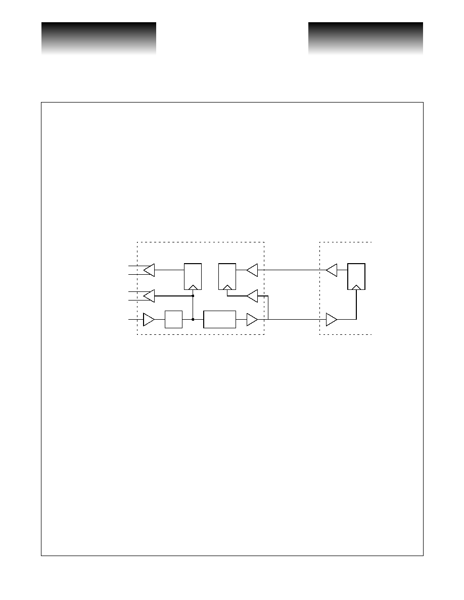
Transmit Section
Byte-wide data is presented to TXIN[7:0] and is clocked into the part on the rising edge of TXLSCKIN.
See Figure 1. The data is then serialized (MSB leading) and presented at the TXDATAOUT+/- pins.
TXDATAOUT is clocked out on the falling edge of TXCLKOUT+. The serial output stream is synchronized to
the CMU generated clock which is a phase locked and frequency scaled version of the input reference clock.
External control inputs B0-B2 and STS-12 select the multiply ratio of the CMU for either STS-3 (155MbS) or
STS-12 (622Mb/s) transmission (see Table 12). A divide-by-8 version of the CMU clock (TXLSCKOUT)
should be used to synchronize the transmit interface of the UNI device to the transmit input registers on the
VSC8113 (see Application Notes, p. 20).
Figure 1: Data and Clock Transmit Block Diagram
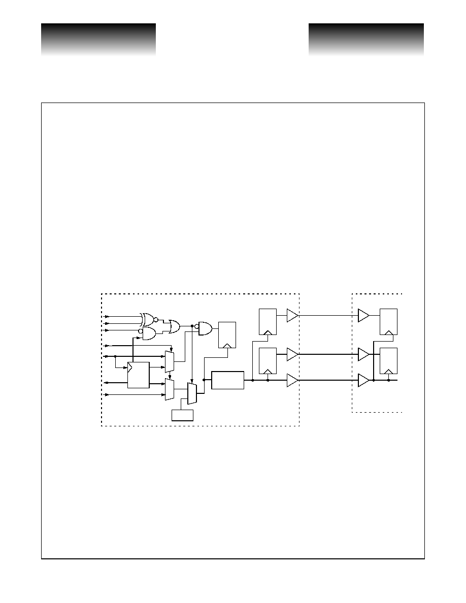
Receive Section
High speed Non-Return to Zero (NRZ) serial data at 155Mb/s or 622Mb/s are received by the RXDATAIN
inputs. The CRU recovers the high speed clock from the serial data input. The serial data is converted to byte-
wide parallel data and presented on RXOUT[7:0] pins. A divide-by-8 version of the high-speed clock
(RXLSCKOUT) should be used to synchronize the byte-serial RXOUT[7:0] data with the receive portion of the
UNI device. The on-chip CRU is by-passed by setting the DSBLCRU input high. In this mode, the serial input
data and corresponding clock are received by the RXDATAIN and RXCLKIN inputs respectively. RXDATAIN
is clocked in on the rising edge of RXCLKIN+. See Figure 2.
The receive section also includes frame detection and recovery circuitry which detects the SONET/SDH
frame, aligns the received serial data on byte boundaries, and initiates a frame pulse on FP coincident with the
byte aligned data. The frame recovery is initiated when OOF is held high which must occur at least 4 byte clock
cycles before the A1A2 boundary. The OOF input control is a level-sensitive signal, and the VSC8113 will con-
tinually perform frame detection and recovery as long as this pin is held high even if 1 or more frames has been
detected. Frame detection and recovery occurs when a series of three A1 bytes followed by three A2 bytes has
been detected. The parallel output data on RXOUT[7:0] will be byte aligned starting on the third A2 byte. When
a frame is detected, a single byte clock period long pulse is generated on FP which is synchronized with the
byte-aligned third A2 byte on RXOUT[7:0]. The frame detector sends a FP pulse only if OOF is high.
D
Q
D
Q
Divide-by-8
CMU
D
Q
TXIN[7:0]
TXLSCKIN
TXLSCKOUT
TXDATAOUT+
TXDATAOUT-
TXCLKOUT+
TXCLKOUT-
REFCLK
VSC8113
PM5355
VITESSE
SEMICONDUCTOR CORPORATION
Data Sheet
VSC8113
ATM/SONET/SDH 622 Mb/s Transceiver Mux/Demux
with Integrated Clock Generation and Clock Recovery
Page 4
©
VITESSE
SEMICONDUCTOR CORPORATION
G52154-0, Rev 4.2
741 Calle Plano, Camarillo, CA 93012 ∑ 805/388-3700 ∑ FAX: 805/987-5896
3/19/99
Loss of Signal
The VSC8113 features Loss of Signal (LOS) detection. Loss of Signal is declared if the incoming serial
data stream has no transition continuously for more than 128 bits. During an LOS condition, the VSC8113
forces the receive data low which is an indication for any downstream equipment that an optical interface failure
has occurred. The receive section continues to be clocked by the CRU as it is now locked to the "CRUREF-
CLK" unless "DSBLCRU" is active in which case it will be clocked by the CMU. This LOS condition will be
removed when the part detects more than 16 transitions in a 128 bit time window. This LOS detection feature
can be disabled by applying a high level to LOSDETEN_ input. The VSC8113 also has a TTL input LOSTTL
and a PECL input LOSPECL to force the part into a Loss of Signal state. Most optics have a PECL output usu-
ally called "SD" or "FLAG" indicating a lack of or presence of optical power. Depending on the optics manu-
factured this signal is either active high or active low. The LOSTTL and LOSPECL inputs are XNOR'd to
generate an internal LOS control signal. See Figure 2. The optics "SD" output should be connected to
LOSPECL. The LOSTTL input should be tied low if the optics "SD" output is active high. If it's active low tie
LOSTTL high. The inverse is true if the optics use "FLAG" for loss of signal.
Figure 2: Data and Clock Receive Block Diagram
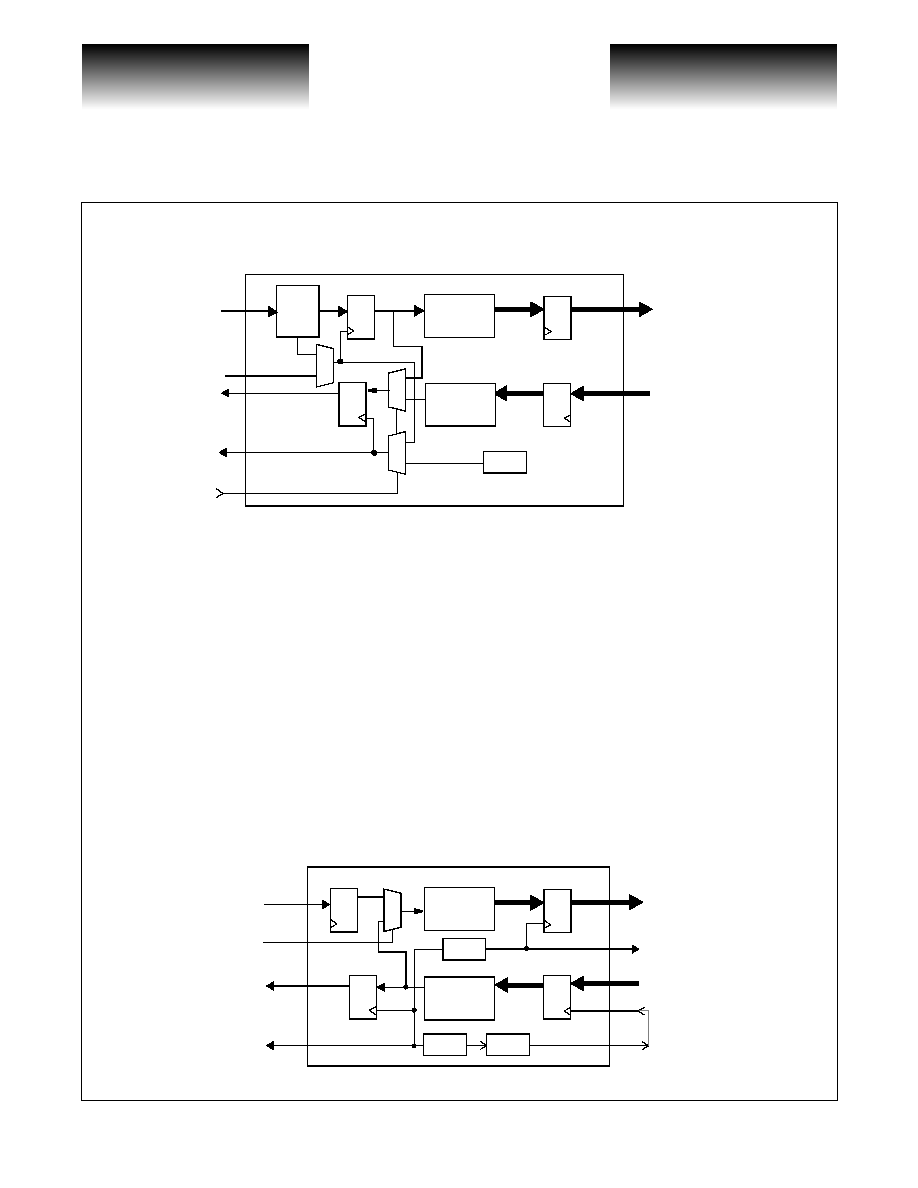
Facility Loopback
The Facility Loopback function is controlled by the FACLOOP signal. When the FACLOOP signal is set
high, the Facility Loopback mode is activated and the high speed serial receive data (RXDATAIN) is presented
at the high speed transmit output (TXDATAOUT). See Figure 3. In addition, the high speed received/recovered
clock is selected and presented at the high speed transmit clock output (TXCLKOUT). In Facility Loopback
mode the high speed receive data (RXDATAIN) is also converted to parallel data and presented at the low speed
receive data output pins (RXOUT[7:0]). The receive clock (RXCLKIN) is also divided down and presented at
the low speed clock output (RXLSCKOUT).
D Q
D Q
D Q
0
1
Divide-by-8
CMU
D Q
PM5355
D Q
RXOUT[7:0]
FP
RXLSCKOUT
VSC8113
CRU
RXDATAIN+/-
RXCLKIN+/-
DSBLCRU
0
1
0
1
CRULOCKDET
LOSTTL
LOSPECL
LOSDETEN_
G52154-0, Rev 4.2
©
VITESSE
SEMICONDUCTOR CORPORATION
Page 5
3/19/99
741 Calle Plano, Camarillo, CA 93012 ∑ 805/388-3700 ∑ FAX: 805/987-5896
VITESSE
SEMICONDUCTOR CORPORATION
Data Sheet
VSC8113
ATM/SONET/SDH 622 Mb/s Transceiver Mux/Demux
with Integrated Clock Generation and Clock Recovery
Figure 3: Facility Loopback Data Path
Equipment Loopback
The Equipment Loopback function is controlled by the EQULOOP signal. When the EQULOOP signal is
set high, the Equipment Loopback mode is activated and the high speed transmit data generated from the paral-
lel to serial conversion of the low speed data (TXIN[7:0]) is selected and converted back to parallel data in the
receiver section and presented at the low speed parallel outputs (RXOUT[7:0]). See Figure 4. The internally
generated 155/622MHz clock is used to generate the low speed receive clock output (RXLSCKOUT). In Equip-
ment Loopback mode the transmit data (TXIN[7:0]) is serialized and presented at the high speed output
(TXDATAOUT) along with the high speed transmit clock (TXCLKOUT) which is generated by the on-chip
clock multiplier unit.
CRU Equipment Loopback
Exactly the same as equipment loopback, the point where the transmit data is looped back is moved all the
way back to the high speed I/O. When the CRUEQLP signal is set high, transmit data is looped back to the
CRU, replacing RXDATAIN±
Figure 4: Equipment Loopback Data Path
D
Q
D
Q
1:8
Serial to
Parallel
Q
D
RXDATAIN
TXDATAOUT
RXOUT[7:0]
Q
D
TXIN[7:0]
8:1
Parallel to
Serial
PLL
0
1
0
1
CRU
TXCLKOUT
FACLOOP
RXCLKIN
0
1
Recovered
Clock
D Q
D
Q
1:8
Serial to
Parallel
Q
D
RXDATAIN
TXDATAOUT
RXOUT[7:0]
Q
D
8:1
Parallel to
Serial
TXIN[7:0]
˜
8
PLL
˜
8
RXLSCKOUT
TXLSCKIN
TXLSCKOUT
TXCLKOUT
0
1
EQULOOP