 | –≠–ª–µ–∫—Ç—Ä–æ–Ω–Ω—ã–π –∫–æ–º–ø–æ–Ω–µ–Ω—Ç: VSC8116QP | –°–∫–∞—á–∞—Ç—å:  PDF PDF  ZIP ZIP |

G52220-0, Rev 4.1
©
VITESSE
SEMICONDUCTOR CORPORATION
Page 1
1/8/00
741 Calle Plano, Camarillo, CA 93012 ∑ 805/388-3700 ∑ FAX: 805/987-5896
VITESSE
SEMICONDUCTOR CORPORATION
Data Sheet
VSC8116
ATM/SONET/SDH 622/155Mb/s Transceiver
Mux/Demux with Integrated Clock Generation
Features
General Description
The VSC8116 is an ATM/SONET/SDH compatible transceiver integrating an on-chip clock multiplication
unit (PLL) for the high speed clock and 8 bit serial-to-parallel and parallel-to-serial data conversion. The high
speed clock generated by the on-chip PLL is selectable for 155.52 or 622.08 MHz operation. The demultiplexer
contains SONET/SDH frame detection and recovery. In addition, the device provides both facility and equip-
ment loopback modes and loop timing modes. The part is packaged in a 64 PQFP with an integrated heat
spreader for optimum thermal performance and reduced cost. The VSC8116 provides an integrated solution for
ATM physical layers and SONET/SDH systems applications.
VSC8116 Block Diagram
∑ Loss of Signal (LOS) Control
∑ Provides Equipment, Facilities and Split Loop-
back Modes as well as Loop Timing Mode
∑ Meets Bellcore, ITU and ANSI Specifications for
Jitter Performance
∑ Single 3.3V Supply Voltage
∑ Low Power - 1.2 Watts Maximum
∑ 64 PQFP Package
∑ Operates at Either STS-3/STM-1 (155.52 Mb/s) or
STS-12/STM-4 (622.08 Mb/s) Data Rates
∑ Compatible with Industry ATM UNI Devices
∑ On Chip Clock Generation of the 155.52 Mhz
or 622.08 Mhz High Speed Clock
∑ Dual 8 Bit Parallel TTL Interface
∑ SONET/SDH Frame Detection and Recovery
D Q
0
1
RXDATAIN+/-
RXCLKIN+/-
0
1
0
1
D
Q
0
1
0
1
8
RXOUT[7:0]
RXLSCKOUT
FP
OOF
EQULOOP
TXDATAOUT+/-
8
TXIN[7:0]
TXLSCKOUT
FACLOOP
LOOPTIM0
CMU
Divide-by-8
1:8
DEMUX
FRAMER
Divide-by-8
8:1
MUX
0
1
D Q
Q D
LOS
LOSTTL
REFCLK

VITESSE
SEMICONDUCTOR CORPORATION
Data Sheet
VSC8116
ATM/SONET/SDH 622/155Mb/s Transceiver
Mux/Demux with Integrated Clock Generation
Page 2
©
VITESSE
SEMICONDUCTOR CORPORATION
G52220-0, Rev 4.1
741 Calle Plano, Camarillo, CA 93012 ∑ 805/388-3700 ∑ FAX: 805/987-5896
1/8/00
Functional Description
The VSC8116 is designed to provide a SONET/SDH compliant interface between the high speed optical
networks and the lower speed User Network Interface (UNI) devices such as the PM5355 S/UNI-622 (or
PM5312 STTX). The VSC8116 transmit section converts 8 bit parallel data at 77.76 Mb/s or 19.44 Mb/s to a
serial bit stream at 622.08 Mb/s or 155.52 Mb/s, respectively. It also provides a Facility Loopback function
which loops the received high speed data and clock directly to the transmit outputs. A Clock Multiplier Unit
(CMU) is integrated into the transmit circuit to generate the high speed clock for the serial output data stream
from input references frequency of 19.44 or 77.76 MHz. The CMU can be bypassed by using the receive clock
in loop timing mode thus synchronizing the entire part to a single clock (RXCLKIN).
The receive section provides the serial-to-parallel conversion, converting 155 Mb/s or 622 Mb/s to an 8 bit
parallel output at 19.44 Mb/s or 77.76 Mb/s, respectively. The receive section provides an Equipment Loopback
function which will loop the low speed transmit data and clock back through the receive section to the 8 bit par-
allel data bus and clock outputs. The receive section also contains a SONET/SDH frame detector circuit which
is used to provide frame recovery in the serial to parallel converter. The block diagram on page 1 shows the
major functional blocks associated with the VSC8116.
Transmit Section
Byte-wide data is presented to TXIN [7:0] and is clocked into the part on the rising edge of TXLSCKOUT
(refer to Figure 1). The data is then serialized (MSB leading) and presented at the TXDATAOUT+/- pins. The
serial output stream is synchronized to the CMU generated clock which is a phase locked and frequency scaled
version of the input reference clock. External control inputs CMUFREQSEL and STS12 select the multiply
ratio of the CMU and either STS-3 (155 Mb/s) or STS-12 (622 Mb/s) transmission (See Table 2).
Figure 1: Data and Clock Transmit Block Diagram
D
Q
D
Q
Divide-by-8
CMU
D
Q
TXIN[7:0]
TXLSCKOUT
TXDATAOUT+
TXDATAOUT-
REFCLK
VSC8116
PM5355

G52220-0, Rev 4.1
©
VITESSE
SEMICONDUCTOR CORPORATION
Page 3
1/8/00
741 Calle Plano, Camarillo, CA 93012 ∑ 805/388-3700 ∑ FAX: 805/987-5896
VITESSE
SEMICONDUCTOR CORPORATION
Data Sheet
VSC8116
ATM/SONET/SDH 622/155Mb/s Transceiver
Mux/Demux with Integrated Clock Generation
Receive Section
High speed Non-Return to Zero (NRZ) serial data at 155Mb/s or 622Mb/s are received by the RXDATAIN
inputs. The corresponding clock is received by the RXCLKIN inputs. RXDATAIN is clocked in on the rising
edge of RXCLKIN+. See Figure 2. The serial data is converted to byte-wide parallel data and presented on
RXOUT[7:0] pins. A divide-by-8 version of the high-speed clock (RXLSCKOUT) should be used to synchro-
nize the byte-serial RXOUT[7:0] data with the receive portion of the UNI device.
The receive section also includes frame detection and recovery circuitry which detects the SONET/SDH
frame, aligns the received serial data on byte boundaries, and initiates a frame pulse on FP coincident with the
byte aligned data. The frame recovery is initiated when OOF is held high which must occur at least 4 byte clock
cycles before the A1A2 boundary. The OOF input control is a level-sensitive signal, and the VSC8116 will con-
tinually perform frame detection and recovery as long as this pin is held high even if 1 or more frames has been
detected. Frame detection and recovery occurs when a series of three A1 bytes followed by three A2 bytes has
been detected. The parallel output data on RXOUT[7:0] will be byte aligned starting on the third A2 byte. When
a frame is detected, a single byte clock period long pulse is generated on FP which is synchronized with the
byte-aligned third A2 byte on RXOUT[7:0]. The frame detector sends an FP pulse only if OOF is high or if a
frame was detected while OOF was being pulled low.
Figure 2: Data and Clock Receive Block Diagram
Loss of Signal
During a LOS condition, the VSC8116 forces the receive data low which is an indication for any downstream
equipment that an optical interface failure has occurred. The receive section is clocked by the transmit section's
D Q
D Q
D Q
0
1
Divide-by-8
CMU
D Q
PM5355
D Q
RXOUT[7:0]
FP
RXLSCKOUT
VSC8116
RXDATAIN+
RXDATAIN-
RXCLKIN+
RXCLKIN-
LOSTTL
1:8 Serial
to Parallel

VITESSE
SEMICONDUCTOR CORPORATION
Data Sheet
VSC8116
ATM/SONET/SDH 622/155Mb/s Transceiver
Mux/Demux with Integrated Clock Generation
Page 4
©
VITESSE
SEMICONDUCTOR CORPORATION
G52220-0, Rev 4.1
741 Calle Plano, Camarillo, CA 93012 ∑ 805/388-3700 ∑ FAX: 805/987-5896
1/8/00
PLL clock multiplier. Optics have either a PECL or TTL output, usually called "SD" (Signal Detect) or "FLAG"
indicating either a lack of or presence of optical power. Depending on the optics manufacture this signal is
either active high or active low polarity. If the optics Signal Detect or FLAG output is a "TTL" signal, it should
be connected to LOSTTL. If it's a "PECL" signal it should be connected through a "PECL" to "TTL" translator
(such as the Motorola "MC100ELT21") which then drives LOSTTL. The follow on part to VSC8116 is the
VSC8117, in this device the signal LOSTTL has been changed to LOSPECL, a PECL input.
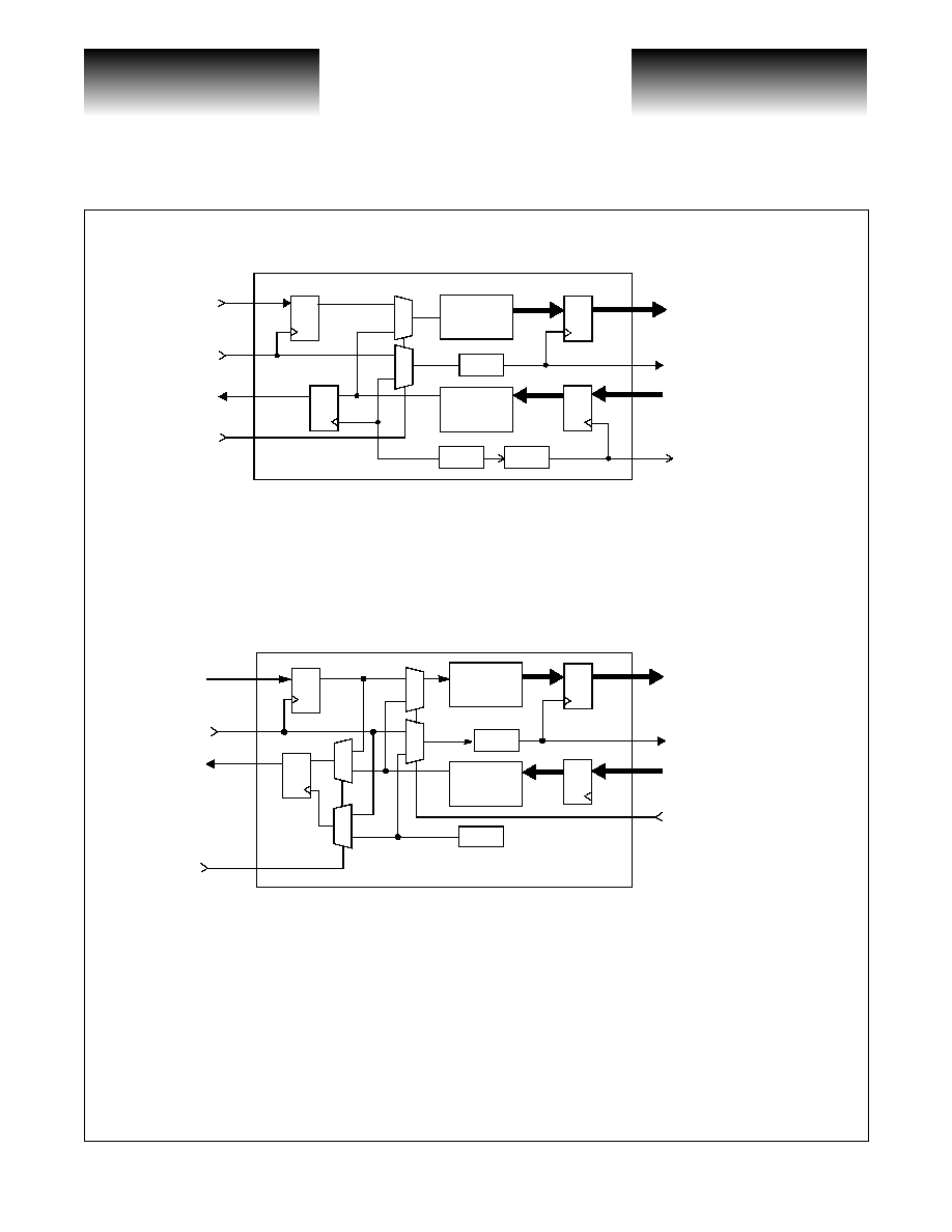
Facility Loopback
The Facility Loopback function is controlled by the FACLOOP signal. When the FACLOOP signal is set
high, the Facility Loopback mode is activated and the high speed serial receive data (RXDATAIN) is presented
at the high speed transmit output (TXDATAOUT). See Figure 3. In Facility Loopback mode the high speed
receive data (RXDATAIN) is also converted to parallel data and presented at the low speed receive data output
pins (RXOUT [7:0]). The receive clock (RXCLKIN) is also divided down and presented at the low speed clock
output (RXLSCKOUT).
Figure 3: Facility Loopback Data Path
Equipment Loopback
The Equipment Loopback function is controlled by the EQULOOP signal. When the EQULOOP signal is
set high, the Equipment Loopback mode is activated and the high speed transmit data generated from the paral-
lel to serial conversion of the low speed data (TXIN [7:0]) is selected and converted back to parallel data in the
receiver section and presented at the low speed parallel outputs (RXOUT [7:0]). See Figure 4. The internally
generated 155MHz/622MHz clock is used to generate the low speed receive clock output (RXLSCKOUT). In
Equipment Loopback mode the transmit data (TXIN [7:0]) is serialized and presented at the high speed output
(TXDATAOUT).
D
Q
D
Q
1:8
Serial to
Parallel
Q
D
RXDATAIN
TXDATAOUT
RXOUT[7:0]
Q
D
TXIN[7:0]
8:1
Parallel to
Serial
PLL
0
1
FACLOOP
RXCLKIN
0
1
RXLSCKOUT
˜
8
G52220-0, Rev 4.1
©
VITESSE
SEMICONDUCTOR CORPORATION
Page 5
1/8/00
741 Calle Plano, Camarillo, CA 93012 ∑ 805/388-3700 ∑ FAX: 805/987-5896
VITESSE
SEMICONDUCTOR CORPORATION
Data Sheet
VSC8116
ATM/SONET/SDH 622/155Mb/s Transceiver
Mux/Demux with Integrated Clock Generation
Figure 4: Equipment Loopback Data Path
Split Loopback
Equipment and facility loopback modes can be enabled simultaneously. See descriptions for equipment and
facility loop modes above. The only change is, since they are both active, RXDATAIN will not be deserialized
and presented to RXOUT[0:7], and TXIN[0:7] will not be serialized and present to TXDATAOUT.
Figure 5: Split Loopback Datapath
Loop Timing
LOOPTIM0 mode bypasses the CMU when the LOOPTIM0 input is asserted high. In this mode the CMU
is bypassed by using the receive clock (RXCLKIN), and the entire part is synchronously clocked from a single
external source.
D Q
D
Q
1:8
Serial to
Parallel
Q
D
RXDATAIN
TXDATAOUT
RXOUT[7:0]
Q
D
8:1
Parallel to
Serial
TXIN[7:0]
˜
8
PLL
˜
8
RXLSCKOUT
TXLSCKOUT
0
1
EQULOOP
0
1
RXCLKIN
D
Q
1:8
Serial to
Parallel
RXOUT[7:0]
Q
D
8:1
Parallel to
Serial
TXIN[7:0]
RXLSCKOUT
D
Q
Q
D
RXDATAIN
TXDATAOUT
0
1
FACLOOP
RXCLKIN
0
1
˜
8
PLL
0
1
EQULOOP
0
1