 | –≠–ª–µ–∫—Ç—Ä–æ–Ω–Ω—ã–π –∫–æ–º–ø–æ–Ω–µ–Ω—Ç: VSC8164 | –°–∫–∞—á–∞—Ç—å:  PDF PDF  ZIP ZIP |

VITESSE
SEMICONDUCTOR CORPORATION
reliminary Datasheet
SC8164
2.488 Gbit/sec to 2.7Gbit/sec
1:16 SONET/SDH Demux
G52239-0, Rev. 3.3
VITESSE
SEMICONDUCTOR CORPORATION
Page 1
5/17/00
741 Calle Plano, Camarillo, CA 93012 ∑ 805/388-3700 ∑ FAX: 805/987-5896
Features
General Description
The VSC8164 is a 1:16 demultiplexer for use in SONET/SDH systems operating at a standard 2.488Gb/s
data rate or forward error correction (FEC) data rate up to 2.7Gb/s. The device operates using a single 3.3V
power supply, and is packaged in a thermally enhanced plastic package. The thermal performance of the
128PQFP allows the use of the VSC8164 without a heat sink under most thermal conditions.
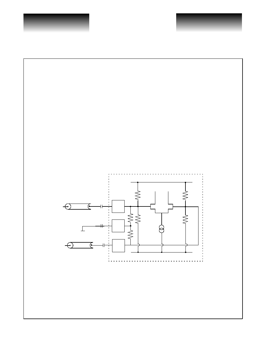
VSC8164 Block DIagram
Functional Description
Low Speed Interface
The demultiplexed serial stream is made available by a 16 bit differential LVPECL interface D[15:0] with
accompanying differential LVPECL divide by 16 clock CLK16O
±
and divide by 32 clock CLK32O
±
. The low
speed LVPECL output drivers are designed to drive a 50
transmission line. The transmission line can be DC
terminated with a split end termination scheme (see Figure 1), or DC terminated by 50
to V
CC
-2V on each line
(see Figure 2). At any time, the equivalent split-end termination technique can be substituted for the traditional
50
to V
CC
-2V on each line. AC coupling can be achieved by a number of methods. Figure 3 illustrates an AC
coupling method for the occasion when the downstream device provides the bias point for AC coupling. If the
downstream device were to have internal termination, the line to line 100
resistor may not be necessary. The
divide by 32 output can be used to provide a reference clock for the clock multiplication unit on the VSC8163.
∑ 2.488Gb/s 1:16 Demultiplexer
∑ Targeted for SONET OC-48 / SDH STM-16
Applications
∑ Supports FEC rates up to 2.7Gb/s
∑ Differential LVPECL Low Speed Interface
∑ Single +3.3V Supply
∑ 128 Pin 14x20mm PQFP Package
D0+
D0-
D15+
D15-
CLK16O+
CLK16O-
DI+
DI-
HSCLKI+
HSCLKI-
Ou
t
p
u
t
R
e
g
i
st
e
r
Divide by
16
CLK32O+
CLK32O-
Divide by
2

VITESSE
SEMICONDUCTOR CORPORATION
Preliminary Datasheet
VSC8164
2.488 Gbit/sec to 2.7Gbit/sec
1:16 SONET/SDH Demux
Page 2
VITESSE
SEMICONDUCTOR CORPORATION
G52239-0, Rev. 3.3
741 Calle Plano, Camarillo, CA 93012 ∑ 805/388-3700 ∑ FAX: 805/987-5896
5/17/00
Figure 1: Split-end DC Termination of Low Speed LVPECL CLK16O, CLK32O, D[15:0] Outputs
Figure 2: Traditional DC Termination of Low Speed LVPECL CLK16O, CLK32O, D[15:0] Outputs
Figure 3: AC Termination of Low Speed LVPECL CLK16O, CLK32O, D[15:0] Outputs
VSC8164
Z
o
Z
o
R2
R2
R1
R1
VEE
VCC
R1||R2 = Z
o
, R1 = 125
R2 = 83
V
CC
R2 + V
EE
R1
R1+R2
= V
Term
downstream
V
CC
-2V
R1 =50
VSC8164
Z
o
V
CC
-2V
R1 =50
downstream
VSC8164
100nF
50
50
Z
o
Z
o
100nF
V
CC
-2V
downstream
bias point
generated
internally
VITESSE
SEMICONDUCTOR CORPORATION
reliminary Datasheet
SC8164
2.488 Gbit/sec to 2.7Gbit/sec
1:16 SONET/SDH Demux
G52239-0, Rev. 3.3
VITESSE
SEMICONDUCTOR CORPORATION
Page 3
5/17/00
741 Calle Plano, Camarillo, CA 93012 ∑ 805/388-3700 ∑ FAX: 805/987-5896
High Speed Interface
The incoming 2.488Gb/s data (up to 2.7Gb/s for FEC applications) and input clock are received by high
speed inputs DI and HSCLKI. The data and clock inputs are internally terminated by a center-tapped resistor
network. For differential input DC coupling, the network is terminated to the appropriate termination voltage
V
Term
(pins HSDREF, HSCLKREF) providing a 50
to
V
Term
termination for both true and complement inputs.
For differential input AC coupling, the network is terminated to
V
Term
via a blocking capacitor.
In most situations these inputs will have high transition density and little DC offset. However, in cases
where this does not hold, direct DC connection is possible. All serial data and clock inputs have the same circuit
topology, as shown in Figure 4. The reference voltage is created by a resistor divider as shown. If the input sig-
nal is driven differentially and DC-coupled to the part, the mid-point of the input signal swing should be cen-
tered about this reference voltage and not exceed the maximum allowable amplitude (
V
CMI
,
V
IHSDC
)
. For
single-ended, DC-coupling operations, it is recommended that the user provides an external reference voltage
which has better temperature and power supply noise rejection than the on-chip resistor divider. The external
reference should have a nominal value equivalent to the common mode switch point of the DC coupled signal,
and can be connected to either side of the differential gate.
Figure 4: High Speed Serial Clock and Data Inputs
Supplies
This device is specified as a LVPECL device with a single positive 3.3V supply. Should the user desire to
use the device in a ECL environment with a negative 3.3V supply, then VCC will be ground and VEE will be -
3.3V.
V
CC
= 3.3V
V
EE
= 0V
C
IN
Chip Boundary
C
IN
TYP = 100 nF
C
AC
TYP = 100 nF
Z
O
V
Term
C
AC
50
50
C
IN
Z
O

VITESSE
SEMICONDUCTOR CORPORATION
Preliminary Datasheet
VSC8164
2.488 Gbit/sec to 2.7Gbit/sec
1:16 SONET/SDH Demux
Page 4
VITESSE
SEMICONDUCTOR CORPORATION
G52239-0, Rev. 3.3
741 Calle Plano, Camarillo, CA 93012 ∑ 805/388-3700 ∑ FAX: 805/987-5896
5/17/00
Decoupling of the power supplies is a critical element in maintaining the proper operation of the part. It is
recommended that the V
CC
power supply be decoupled using a 0.1
µ
F and 0.01
µ
F capacitor placed in parallel
on each V
CC
power supply pin as close to the package as possible. If room permits, a 0.001
µ
F capacitor should
also be placed in parallel with the 0.1
µ
F and 0.01
µ
F capacitors mentioned above. Recommended capacitors are
low inductance ceramic SMT X7R devices. For the 0.1
µ
F capacitor, a 0603 package should be used. The
0.01
µ
F and 0.001
µ
F capacitors can be either 0603 or 0402 packages.
For low frequency decoupling, 47
µ
F tantalum low inductance SMT caps should be sprinkled over the
board's main +3.3V power supply and placed close to the C-L-C pi filter.
If the device is being used in an ECL environment with a -3.3V supply, then all references to decoupling
V
CC
must be changed to V
EE
, and all references to decoupling 3.3V must be changed to -3.3V.
AC Characteristics
Figure 5: AC Timing Waveforms
Figure 6: High Speed Input Timing
VALID DATA (1)
VALID DATA (2)
Parallel data clock output
Parallel data outputs
Parallel data clock output
CLK16O+
D(0...15)+
CLK32O+
t
pdd
t
pd32
D0
D1 D2
D3
D4 D5 D6 D7 D8 D9 D10D11 D12
High speed differential clock input
High speed differential serial data input
HSCLKI+
DI+
t
dsu
t
dh
D13D14 D15

VITESSE
SEMICONDUCTOR CORPORATION
reliminary Datasheet
SC8164
2.488 Gbit/sec to 2.7Gbit/sec
1:16 SONET/SDH Demux
G52239-0, Rev. 3.3
VITESSE
SEMICONDUCTOR CORPORATION
Page 5
5/17/00
741 Calle Plano, Camarillo, CA 93012 ∑ 805/388-3700 ∑ FAX: 805/987-5896
Figure 7: Differential and Single Ended Input and Output Voltage Measurement
Table 1: AC Characteristics
Parameters
Description
Min
Max
Units
Conditions
t
pdd
Data valid from falling
edge of CLK16O+
0
800
ps.
t
pd32
CLK32O transition from
falling edge of CLK16O+
0
1.0
ns.
t
DR
, t
DF
D[15:0]+/- rise and fall
times
--
400
ps
20% to 80% into 50 Ohm load.
See Figure 7
t
CLKR
, t
CLKF
CLK16O+/- rise and fall
times
--
250
ps
20% to 80% into 50 Ohm load.
See Figure 7
CLK16O
D
CLK16O+/- duty cycle
distortion
45
55
% of
clock
cycle
High speed clock input at 2.488GHz
t
dsu
DI+ setup time with respect
to falling edge of
HSCLKI+
100
--
ps
t
dh
DI+ hold time with respect
to falling edge of
HSCLKI+
75
--
ps
HSCLKI
D
HSCLKI+/- duty cycle
distortion
40
60
% of
clock
cycle
Single
Ended
Swing
Differential
Swing
=
=
a
a
b
b
* Differential swing
(
) is specified as | b - a | ( or | a - b | ), as is the single ended swing.
Differential swing is specified as equal in magnitude to single ended swing.