 | –≠–ª–µ–∫—Ç—Ä–æ–Ω–Ω—ã–π –∫–æ–º–ø–æ–Ω–µ–Ω—Ç: VSC837UG | –°–∫–∞—á–∞—Ç—å:  PDF PDF  ZIP ZIP |

VITESSE
SEMICONDUCTOR CORPORATION
Preliminary Data Sheet
VSC837
3.2Gb/s
68x68 Crosspoint Switch
G52309-0, Rev 3.0
Page 1
02/16/01
© VITESSE
SEMICONDUCTOR CORPORATION ∑ 741 Calle Plano ∑ Camarillo, CA 93012
Tel: (800) VITESSE ∑ FAX: (805) 987-5896 ∑ Email: prodinfo@vitesse.com
Internet: www.vitesse.com
Features
General Description
The VSC837 is a monolithic 68x68 asynchronous crosspoint switch, designed to carry broadband data
streams. The non-blocking switch core is programmed through a triple-mode port interface that allows random
access programming of each input/output port. A high degree of signal integrity is maintained throughout the
chip via fully differential signal paths.
The crosspoint function is based on a multiplexer array architecture. Each data output is driven by a 68:1
multiplexer that can be programmed to one and only one of its 68 inputs. The signal path is unregistered and
fully asynchronous, so there are no restrictions on the phase, frequency, or signal pattern at each input.
Each high-speed output is a fully differential switched current driver with switchable on-die terminations
for maximum signal integrity. Data inputs are terminated on die through 100
resistors between true and com-
plement inputs (see Input Termination section for further detail).
A triple-mode programming interface is provided that allows programming commands to be sent as serial
data or one of two forms of parallel data. The input-referred mode (burst mode) allows an input port to be routed
to all outputs in only 4 program cycles. Core programming can be random for each port address, or multiple
program assignments can be queued and issued simultaneously. The programming may be initialized to a
"straight-through" configuration (A0 to Y0, A1 to Y1, etc.) using the INITB pin.
An activity monitor is provided to allow in-system diagnostics. The activity monitor can observe any high-
speed input via an internal 69th multiplexer.
Unused channels may be powered down to allow efficient use of the switch in applications that require only
a subset of the channels. Power-down can be accomplished in hardware, via dedicated power pins for pairs of
input and output channels, or in software by programming individual unused outputs with a disable code.
VSC837 Block Diagram
∑ 68 Input by 68 Output Crosspoint Switch
∑ 3.2Gb/s NRZ Data Bandwidth
∑ 66MHz Multi-Mode Programming Port
∑ TTL/2.5V CMOS Control I/O (3.3V tolerant)
∑ Programmable On-Chip I/O Termination
∑ Input Signal Activity (ISA) Monitoring Function
∑ Integrated Signal Equalization (ISE) for
Deterministic Jitter Reduction
∑ Single 2.5V Supply
∑ Differential CML Output Driver
∑ 11W typ/14W max (low drive mode)
13W typ/16W max (high drive mode)
∑ Hard and Soft Power-Down for Unused Channels
∑ High Performance 37.5mm, 480 TBGA Package
2
2
2
2
A0
A67
Y0
Y67
µ
P
control

VITESSE
SEMICONDUCTOR CORPORATION
Preliminary Data Sheet
VSC837
3.2Gb/s
68x68 Crosspoint Switch
Page 2
G52309-0, Rev 3.0
02/16/01
© VITESSE
SEMICONDUCTOR CORPORATION ∑ 741 Calle Plano ∑ Camarillo, CA 93012
Tel: (800) VITESSE ∑ FAX: (805) 987-5896 ∑ Email: prodinfo@vitesse.com
Internet: www.vitesse.com
Functional Block Diagram
Functional Description
Input / Output Characteristics
All input data must be differential and should be nominally biased to +2.0V or AC-coupled. Other levels
are allowed as described under the Input Termination section. On-chip terminations are provided, with a nomi-
nal impedance of 100
differential. All input termination resistors float with an internal bias provided for AC-
coupling.
For direct interconnection of multiple VSC837 devices, a CML termination mode is provided by tying the
ITC pin to V
CC
, which ties the center point of the 100
termination to V
CC
, causing the terminations to act as
loads for an open-drain or open-collector differential output.
Data outputs are provided through differential current switches with on-chip back-termination. The output
circuit is capable of driving external 50
far-end termination (recommended). The output back-terminations are
electronically switchable to enable a power savings of 2W (max) by reducing the output driver current.
68x69 Switch Core
Core Program Registers
CONFIG
INITB
Internal 69
th
Output
A, AN[0:67]
SDOUT
SERIAL
B
URST
CSB
LO
AD
ALE_SCN
Y, YN[0:67]
OUTCHAN[18:0]
INCHAN[6:0]
Program Memory
Program Interface
A
CTCLK
A
CTIVITY
Activity
Monitor

VITESSE
SEMICONDUCTOR CORPORATION
Preliminary Data Sheet
VSC837
3.2Gb/s
68x68 Crosspoint Switch
G52309-0, Rev 3.0
Page 3
02/16/01
© VITESSE
SEMICONDUCTOR CORPORATION ∑ 741 Calle Plano ∑ Camarillo, CA 93012
Tel: (800) VITESSE ∑ FAX: (805) 987-5896 ∑ Email: prodinfo@vitesse.com
Internet: www.vitesse.com
Programming Interface
Parallel Mode
In parallel mode (SERIAL=0, BURST=0), the binary word on INCHAN[6:0] is the numerical identifier of
the input that will be routed to the specified output. OUTCHAN[6:0] is the numerical identifier of the output
being programmed. A rising edge on the LOAD signal will transfer the programming data to the shadow regis-
ter in the program memory. Raising CONFIG (asynchronously) will transfer the programming data to the main
latches in the program memory and cause the internal select signals in the core to re-configure the multiplexer.
Lowering CONFIG will latch the main latches. CONFIG may be tied HIGH to enable programming take effect
instantaneously.
This interface may be used with multiplexed address/data buses by using only INCHAN[6:0] without
OUTCHAN[6:0] and dropping ALE when the address of the output to be programmed is present on
INCHAN[6:0]. After the address is latched, the input address may be presented on INCHAN[6:0] and pro-
gramming proceeds as above.
No read-back capability is provided in parallel mode. Read-back for diagnostic purposes is provided in
serial mode via the scan function.
Serial Mode
In serial mode (SERIAL=1, BURST=0), the INCHAN0 pin becomes the serial data input and the
INCHAN1 pin becomes the serial clock (rising edge triggered). A serial word of the form [Output][Input] is
shifted into the internal shift register, and the LOAD pin is asserted (HIGH) coincident with the last bit of the
data word to signal that the word is to be applied. This transfers the input identifier to the shadow register of the
addressed output. CONFIG is then applied (asynchronously) to transfer one or more program commands to the
main latches of the program memories.
The SDOUT pin follows the data on the INCHAN0_SDIN pin 14 clock cycles later. This enables the user
to chain the serial ports of several crosspoints, shift program data for all switches through such a chain, and
assert LOAD on all switches simultaneously to program all of the connections simultaneously.
The output field is 7 bits long, representing the binary numerical identifier of the output to be programmed.
The input field is 7 bits long, representing the numerical identifier of the input that will be routed to the speci-
fied output.
Serial Read-Back
Read-back of the program memory contents is accomplished in serial mode by setting the ALE_SCN pin
HIGH. This will serially shift out the contents of the main latches in the program memories, slice 68 first and
slice 0 last, and MSB-first, LSB-last for each 7-bit word. One rising edge of INCHAN1_SCLK with
ALE_SCN=0 and SERIAL=1 must occur to load the entire 483-bit shift register prior to shifting out data. At a
clock rate of 66MHz, this operation takes 7.26
µ
s.

VITESSE
SEMICONDUCTOR CORPORATION
Preliminary Data Sheet
VSC837
3.2Gb/s
68x68 Crosspoint Switch
Page 4
G52309-0, Rev 3.0
02/16/01
© VITESSE
SEMICONDUCTOR CORPORATION ∑ 741 Calle Plano ∑ Camarillo, CA 93012
Tel: (800) VITESSE ∑ FAX: (805) 987-5896 ∑ Email: prodinfo@vitesse.com
Internet: www.vitesse.com
Burst Mode
Burst mode programming (BURST=1, SERIAL=0) enables an input to be broadcast to any group of 1 to 17
outputs with a single command. In this mode, rising edges on the LOAD pin will trigger program operations.
The INCHAN[6:0] pins represent the input to be broadcast. The OUTCHAN[18:17] pins represent the page
(quarter) of the program memory to access, and each of the OUTCHAN[16:0] pins represents 1 of the 17 out-
puts within that page. A '1' on any of those pins will cause that output to be programmed to connect to the input
named on INCHAN[6:0].
No read-back capability is provided in burst mode. See Serial Read-Back section above.
Activity Monitoring
The activity monitor observes the output of the internal 69th output from the core. By programming the
69th output to observe various inputs, the input signals can be scanned for activity or lack thereof. Each rising
edge of ACTCLK causes the monitor to read out the activity state from the previous ACTCLK period and clears
the internal activity state until a data transition triggers it again. There must be a minimum of one rising and one
falling edge on the observed input data pin during the ACTCLK period for activity to be detected. After power-
on the output of ACTIVITY after the first ACTCLK rising edge is unknown.
Selective Power-Down
Unused input and output channels can be made to consume little or no power via one of two methods of
selective power-down.
Software Power-Down
Using this feature, unused outputs may be disabled, saving approximately 170 mW per channel for maxi-
mum dissipation conditions. This is accomplished by programming each unused output to look at input 127 (7F
Hex), which represents a non-existent input channel. The channel may be subsequently activated by program-
ming a valid input address. It is recommended, however, that any changes in power programming only be exe-
cuted as part of an initialization sequence to guard against the effects of any switching transients that might
result from changing the power supply current suddenly. Software mode does not affect the functioning or
power of unused input channels.
Hardware Power-Down
Using this feature, the power associated with given pairs of inputs may be shut off by tying the correspond-
ing V
EE
pin to V
CC
(see Table 10). Approximately 160 mW per input pair is saved under the maximum dissipa-
tion conditions. The power associated with given pairs of outputs, including their contribution to the core
power, can be shut off by tying the corresponding V
EE
pin to V
CC
(see Table 10). Approximately 360 mW per
output pair is saved under the maximum dissipation conditions.
Certain V
EE
pins must always be active. In other words, tied to the most negative supply, so the correspond-
ing inputs and outputs will always be on and consuming power. See Figure 6 and Table 10 for the location of
these pins.
VITESSE
SEMICONDUCTOR CORPORATION
Preliminary Data Sheet
VSC837
3.2Gb/s
68x68 Crosspoint Switch
G52309-0, Rev 3.0
Page 5
02/16/01
© VITESSE
SEMICONDUCTOR CORPORATION ∑ 741 Calle Plano ∑ Camarillo, CA 93012
Tel: (800) VITESSE ∑ FAX: (805) 987-5896 ∑ Email: prodinfo@vitesse.com
Internet: www.vitesse.com
AC Characteristics
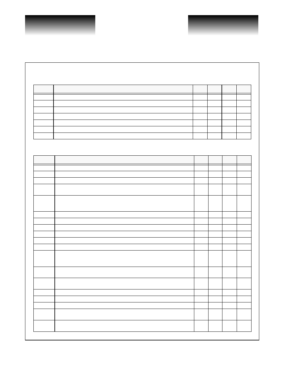
Table 1: Data Path
NOTES:(1) Tested on a sample basis only. (2) Broadband (unfiltered) deterministic jitter added to a jitter-free input, 2
23
-1 PRBS data pattern.
Table 2: Program Interface Timing
Symbol
Parameter
Min
Typ
Max
Units
f
RATE
Maximum Data Rate
--
--
3.2
Gb/s
t
SKW
Channel-to-channel delay skew
--
300
--
ps
t
PDAY
Propagation Delay from an A input to a Y output
--
750
--
ps
t
R
, t
F
High-speed input rise/fall times, 20% to 80%
--
--
150
ps
t
R
, t
F
High-speed output rise/fall times, 20% to 80%
--
--
150
ps
t
JR
Output added delay jitter, rms
(1, 2)
--
--
10
ps
t
JP
Output added delay jitter, peak-to-peak
(1, 2)
--
--
40
ps
Symbol
Parameter
Min
Typ
Max
Units
t
sWRB
Setup time from INCHAN[6:0] or OUTCHAN[6:0] to rising edge of WRB
3.35
--
--
ns
t
hWRB
Hold time from rising edge of WRB to INCHAN[6:0] or OUTCHAN[6:0]
1.45
--
--
ns
t
pwLW
Pulse width (HIGH or LOW) on LOAD
6.75
--
--
ns
t
sCSB
Setup time from CSB to falling edge of LOAD or ALE_SCN in parallel or burst
mode, or rising edge of LOAD in serial mode.
0
--
--
ns
t
hCSB
Hold time of CSB rising edge after LOAD or ALE_SCN rising in parallel or
burst mode, or falling edge of LOAD in serial mode, or falling edge of CONFIG
in any mode.
0
--
--
ns
t
pwCFG
Pulse width (HIGH or LOW) on CONFIG
6.75
--
--
ns
t
sSDIN
Setup time from INCHAN0_SDIN to INCHAN1_SCLK rising
1.65
--
--
ns
t
hSDIN
Hold time of INCHAN0_SDIN after INCHAN1_SCLK rising
1.0
--
--
ns
t
perSCLK
Minimum period of SCLK in serial mode
15
--
--
ns
t
sLOAD
Setup time from LOAD to INCHAN1_SCLK rising
1.85
--
--
ns
t
hLOAD
Hold time of LOAD after INCHAN1_SCLK rising
0.95
--
--
ns
t
sSERIAL
Setup time from SERIAL rising to INCHAN1_SCLK rising when entering serial
mode or SERIAL falling to LOAD falling when entering parallel mode or
SERIAL falling to LOAD rising when entering burst mode.
0.90
--
--
ns
t
hSERIAL
Hold time from INCHAN1_SCLK rising to SERIAL falling when exiting serial
mode.
0
--
--
ns
t
sBURST
Setup time from BURST rising to LOAD rising when entering burst mode or
BURST falling to LOAD falling when entering parallel mode.
1.85
--
--
ns
t
hBURST
Hold time from LOAD rising to BURST falling when exiting burst mode.
2.45
--
--
ns
t
dsDOUT
Delay from INCHAN1_SCLK rising to SDOUT, 20pF load.
--
--
6.20
ns
t
pwINITB
Pulse width (HIGH or LOW) on INITB
6.75
--
--
ns
t
sSCAN
Setup time from ALE_SCN to INCHAN1_SCLK rising when starting or
completing a serial read-back sequence.
1.65
--
--
ns
t
hSCAN
Hold time of ALE_SCN after INCHAN1_SCLK rising when starting or
completing a serial read-back sequence.
1.0
--
--
ns