Document :1G5-0177
Rev.2
Page 1
VIS
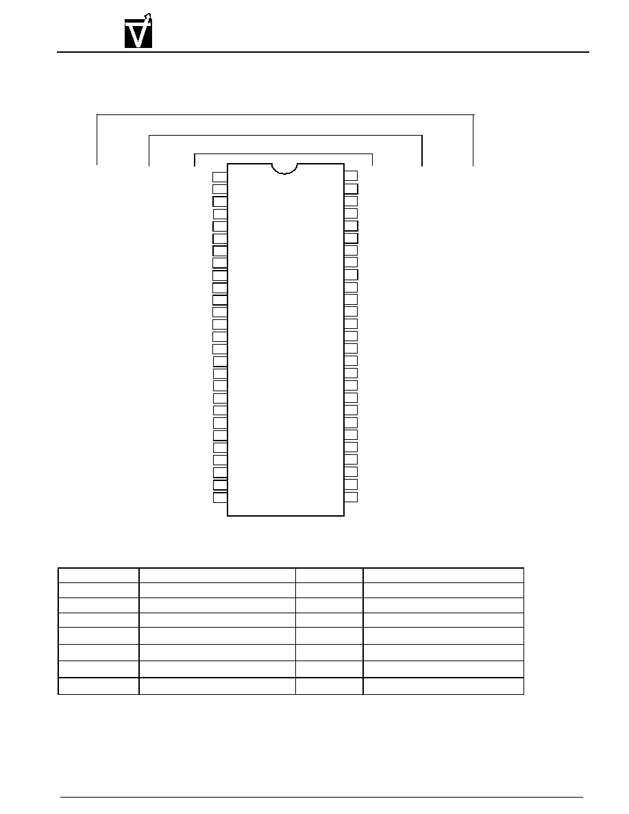
VG36644041DT / VG36648041DT / VG36641641DT
CMOS Synchronous Dynamic RAM
Description
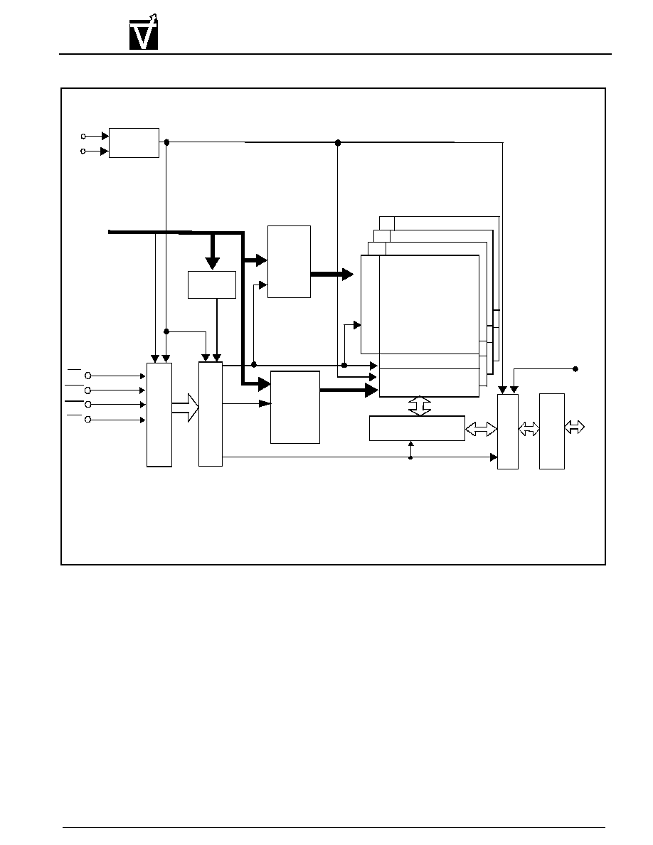
The VG36644041D, VG36648041D and VG36641641D are high-speed 67,108,864-bit synchronous
dynamic random-access memories, organized as 4,194,304 x 4 x 4, 2,097,152 x 8 x 4 and 1,048,576 x 16 x
4 (word x bit x bank), respectively.
The synchronous DRAMs achieved high-speed data transfer using the pipeline architecture. All input
and outputs are synchronized with the positive edge of the clock.The synchronous DRAMs are compatible
with Low Voltage TTL (LVTTL).These products are packaged in 54-pin TSOPII.
Features
· Single 3.3V (
) power supply
· High speed clock cycle time
-6 : 166MHz<3-3-3>, available only on 4MX16 option
-7 : 143MHz<3-3-3>, 133MHz<2-3-2>
-7L: 133MHz<3-3-3>
-8H: 100MHz<2-2-2>
· Fully synchronous operation referenced to clock rising edge
· Possible to assert random column access in every cycle
· Quad internal banks controlled by A12 & A13 (Bank Select)
· Byte control by LDQM and UDQM for VG36641641D
· Programmable Wrap sequence (Sequential / Interleave)
· Programmable burst length (1, 2, 4, 8 and full page)
· Programmable /CAS latency (2 and 3)
· Automatic precharge and controlled precharge
· CBR (Auto) refresh and self refresh
· X4, X8, X16 organization
· LVTTL compatible inputs and outputs
· 4,096 refresh cycles / 64ms
· Burst termination by Burst stop and Precharge command
0.3V
±
Document :1G5-0177
Rev.2
Page 4
VIS
VG36644041DT / VG36648041DT / VG36641641DT
CMOS Synchronous Dynamic RAM
Pin Function
Symbol
Input
Function
CLK
Input
Maste Clock: Other inputs signals are referenecd to the CLK rising edge
CKE
Input
Clock Enable: CKE HIGH activates, and CKE LOW deactivates internal clock signals,
device input buffers and output drivers. Deactivating the clock provides PRECHARGE
POWER-DOWN and SELF REFRESH operation (all banks idle), or ACTIVE POWER-
DOWN (row ACTIVE in any bank).
/CS
Input
Chip Select: CS# enables (registered LOW) and disables (registered HIGH) the com-
mand decoder. All commands are masked when CS# is registered HIGH. CS# provides
for external bank selection on systems with multiple banks. CS# is considered part of
the command code.
/RAS, /CAS,
/WE
Input
Command Inputs: RAS#, CAS# and WE# (along with CS#) define the command being
entered.
A0 - A13
Input
Address Inputs: Provide the row address for ACTIVE commands, and the column
address and AUTO PRECHARGE bit for READ/WRITE commands, to select one loca-
tion out of the memory array in the respective bank.
The row address is specified by A0-A11.
The column address is specified by A0-A9 (X4) / A0-A8 (X8) / A0-A7 (X16)
BA0,BA1
Input
Bank Address Inputs: BA0 and BA1 define to which bank an ACTIVE, READ, WRITE or
PRECHARGE command is being applied.
DQM, UDQM ,
LDQM
Input
Address Inputs: Provide the row address for ACTIVE commands (row address A0-
A10), and the column address and AUTO PRECHARGE bit for READ/WRITE com-
mands (column address A0-A7 with A10 defining AUTO PRECHARGE), to select one
location out of the memory array in the respective bank.
DQ0 - DQ15
I/O
Data Input / Output: Data bus
V
DD,
V
SS
Supply
Power Supply for the memory array and peripheral circuitry
V
DDQ,
V
SSQ
Supply
Power Supply are supplied to the output buffers only

Document :1G5-0177
Rev.2
Page 5
VIS
VG36644041DT / VG36648041DT / VG36641641DT
CMOS Synchronous Dynamic RAM
Absolute Maximum Rating
s
Caution
Exposing the device to stress above those listed in Absolute Maximum Ratings could cause permanent damage. The
device is not meant to be operated under conditions outside the limits described in the operational section of this
specification. Exposure to Absolute Maximum Rating conditions for extended periods may affect device reliability.
Parameter
Symbol
Conditions
Value
Unit
Supply Voltage
V
DD
with respect to V
SS
-0.5 to 4.6
V
Supply Voltage for Output
V
DDQ
with respect to V
SSQ
-0.5 to 4.6
V
Input Voltage
V
I
with respect to V
SS
-0.5 to V
DD
+0.5
V
Output Voltage
V
O
with respect to V
SSQ
-0.5 to V
DDQ
+0.5
V
Short circuit output current
I
O
50
mA
Power dissipation
P
D
T
a
= 25 °C
1
W
Operating temperature
T
OPT
0 to 70
°C
Storage temperature
T
STG
-65 to 150
°C
Recommended Operating Conditions (T
a
= 0 ~ 70 °C, unless otherwise noted)
Parameter
Symbol
Limits
Unit
Min.
Typ.
Max.
Supply Voltage
V
DD
3.0
3.3
3.6
V
Supply Voltage for DQ
V
DDQ
0
0
0
V
Ground
V
SS
3.0
3.3
3.6
V
Ground for DQ
V
SSQ
0
0
0
V
High Level Input Voltage (all inputs)
V
IH
2.0
V
DD
+ 0.3
V
Low Level Input Voltage (all inputs)
V
IL
-0.3
0.8
V
Pin Capacitance (Ta = 0 ~ 70°C, V