 | Рлектронный компонент: 68020 | Скачать:  PDF PDF  ZIP ZIP |
1
White Microelectronics · Phoenix, AZ · (602) 437-1520
WC32P020-XXM
68020 FEATURES
s Selection of Processor Speeds: 16.67, 20, 25 MHz
s Military Temperature Range: -55
°
C to +125
°
C
s Packaging
· 114 pin Ceramic PGA (P2)
· 132 lead Ceramic Quad Flatpack, CQFP (Q2)
s Object-code compatible with earlier 68000 Microprocessors
s Addressing mode extensions for enhanced support of high-
level languages
s Bit Field Data Type Accelerates Bit-Oriented Applications
i.e., Video Graphics
s Fast On-Chip Instruction Cache Speeds Instructions and
Improves Bus Bandwidth
s Coprocessor Interface to Companion 32-Bit Peripheralsthe
68881 and 68882 Floating-Point Coprocessors and the 68851
Paged Memory Management Unit
s Pipelined Architecture with High Degree of Internal
Parallelism allowing Multiple Instructions to be executed
concurrently
December 1998
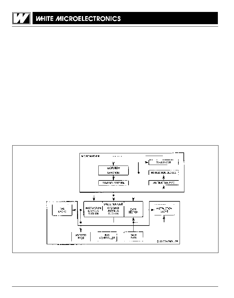
FIG. 1
BLOCK DIAGRAM
s High-Performance Asynchronous Bus Is Nonmultiplexed and
Full 32-Bits
s Dynamic Bus Sizing Efficiently Supports 8-/16-/32-Bit
Memories and Peripherals
s Full Support of Virtual Memory and Virtual Machine
s 16 32-Bit General-Purpose Data and Address Registers
s Two 32-Bit Supervisor Stack Pointers and Five Special-
Purpose Control Registers
s 18 Addressing Modes and 7 Data Types
s 4 GigaByte Direct Addressing Range
DESCRIPTION
The WC32P020 is a 32-bit implementation of the 68000 Family
of microprocessors. Using HCMOS technology, the WC32P020
is implemented with 32-bit registers and data paths, 32-bit
addresses, a powerful instruction set, and flexible addressing
modes.

2
White Microelectronics · Phoenix, AZ · (602) 437-1520
FIG. 2
PIN CONFIGURATION FOR WC32P020-XXM, CQFP (Q2)
18
19
20
21
22
23
24
25
26
27
28
29
30
31
32
33
34
35
36
37
38
39
40
41
42
43
44
45
46
47
48
49
50
17
16
15
14
13
12
11
10
9
8
7
6
5
4
3
2
1
132
131
130
129
128
127
126
125
124
123
122
121
120
119
118
117
NC
BGAC
BR
A
0
A
1
A
31
A
30
A
29
A
28
A
27
A
26
A
25
A
24
A
23
A
22
A
21
A
20
A
19
A
18
A
17
V
DD
V
DD
GND
GND
A
16
A
15
A
14
A
13
A
12
A
11
A
10
NC
NC
NC
NC
NC
A
9
A
8
A
7
A
6
A
5
A
4
A
3
A
2
GND
OSC
IPEND
V
DD
V
DD
GND
GND
IPL
2
IPL
1
IPL
0
D
0
D
1
D
2
D
3
D
4
GND
GND
V
DD
V
DD
D
5
NC
NC
NC
D
31
D
30
D
29
D
28
D
27
D
26
D
25
D
24
D
23
D
22
D
21
D
20
D
19
D
18
D
17
D
16
GND
GND
V
DD
V
DD
D
15
D
14
D
13
D
12
D
11
D
10
D
9
D
8
D
7
D
6
NC
NC
NC
NC
GND
BG
V
DD
GND
GND
CLK
RESET
V
DD
V
DD
RMC
FC
0
FC
1
FC
2
SIZ
0
SIZ
1
DBEN
ECS
CDIS
AVEC
DSACK
0
DSACK
1
BERR
GND
GND
HALT
AS
DS
GND
GND
R/W
NC
51
52
53
54
55
56
57
58
59
60
61
62
63
64
65
66
67
68
69
70
71
72
73
74
75
76
77
78
79
80
81
82
83
116
115
114
113
112
111
110
109
108
107
106
105
104
103
102
101
100
99
98
97
96
95
94
93
92
91
90
89
88
87
86
85
84
WC32P020-XXM
FIG. 3
PIN CONFIGURATION FOR WC32P020-XXM, PGA (P2)
TOP VIEW
D
31
DS
AS
GND
CDIS
ECS
SIZ
0
FC
0
V
CC
RESET
GND
BGACK
1 2 3 4 5 6 7 8 9 10 11 12 13
D
28
D
29
R/W
HALT
BERR
AVEC
SIZ
1
FC
2
RMC
V
CC
CLK
BG
A
1
DSACK
1
D
25
D
26
D
30
GND
GND
DSACK
0
DBEN
FC
1
V
CC
V
CC
GND
BR
A
31
D
22
D
24
D
27
A
0
A
30
A
28
D
20
D
21
D
23
A
29
A
27
A
26
D
17
D
18
D
19
A
25
A
24
A
23
GND
D
16
GND
A
21
A
20
A
22
V
CC
V
CC
D
15
A
17
A
18
A
19
D
14
D
13
D
11
A
16
GND
V
CC
D
12
D
10
D
7
A
12
D
15
GND
D
9
D
6
GND
A
9
D
13
A
14
D
8
D
5
D
3
D
1
IPL
0
IPL
2
GND
GND
A
2
A
4
A
7
A
10
A
11
V
CC
D
4
D
2
D
0
IPL
1
GND
V
CC
IPEND
OCS
A
3
A
5
A
6
A
8
V
CC
N
M
L
K
J
H
G
F
E
D
C
B
A

3
White Microelectronics · Phoenix, AZ · (602) 437-1520
WC32P020-XXM
ADDRESSING MODES
Addressing
Syntax
Register Direct
Data Register Direct
Dn
Address Register Direct
An
Register Indirect
Address Register Indirect
(An)
Address Register Indirect with Postincrement
(An) +
Address Register Indirect with Predecrement
- (An)
Address Register Indirect with Displacement
(d
16
,An)
Register Indirect with Index
Address Register Indirect with Index (8-Bit Displacement)
(d
8
,An,Xn)
Address Register Indirect with Index (Base Displacement)
(bd,An,Xn)
Memory Indirect
Memory Indirect Postindexed
([bd,An],Xn,od)
Memory Indirect Preindexed
([bd,An,Xn],od)
Program Counter Indirect with Displacement
(d
16
,PC)
Program Counter Indirect with Index
PC Indirect with Index (8-Bit Displacement)
(d
8
,PC,Xn)
PC Indirect with Index (Base Displacement)
(bd,PC,Xn)
Program Counter Memory Indirect
PC Memory Indirect Postindexed
([bd,PC],Xn,od)
PC Memory Indirect Preindexed
([bd,PC,Xn],od)
Absolute
Absolute Short
(xxx).W
Absolute Long
(xxx).L
Immediate
#(data)
NOTES:
Dn = Data Register, DO-D7
An = Address Register, AO-A7
d
8
, d
16
= A twos-complement or sign-extended displacement; added as part
of the effective address calculation; size is 8 (d8) or 16 (d16) bits;
when omitted, assemblers use a value of zero.
Xn = Address or data register used as an index register; form is
Xn.SIZE*SCALE, where SIZE is.W or .L (indicates index register size)
and SCALE is 1, 2, 4, or 8 (index register is multiplied by SCALE);
use of SIZE and/or SCALE is optional.
bd = A twos-complement base displacement; when present, size can be
16 or 32 bits.
od = 0uter displacement, added as part of effective address calculation
after any memory indirection, use is optional with a size of 16 or 32
bits.
PC = Program Counter
(data) = Immediate value of 8, 16, or 32 bits
( ) = Effective Address
[ ] = Use as indirect access to long-word address.
Mnemonic
Description
Bcc
Branch Conditionally
BCHG
Test Bit and Change
BCLR
Test Bit and Clear
BFCHG
Test Bit Field and Change
BFCLR
Test Bit Field and Clear
BFEXTS
Signed Bit Field Extract
BFEXTU
Unsigned Bit Field Extract
BFFFO
Bit Field Find First One
BFINS
Bit Field Insert
BFSET
Test Bit Field and Set
BFTST
Test Bit Field
BKPT
Breakpoint
BRA
Branch
BSET
Test Bit and Set
BSR
Branch to Subroutine
BTST
Test Bit
CALLM
Call Module
CAS
Compare and Swap Operands
CAS2
Compare and Swap Dual
Operands
CHK
Check Register Against Bound
CHK2
Check Register Against Upper and Lower Bounds
CLR
Clear
CMP
Compare
CMPA
Compare Address
CMPI
Compare Immediate
CMPM
Compare Memory to Memory
CMP2
Compare Register Against Upper and Lower Bounds
DBcc
Test Condition, Decrement and Branch
DIVS, DIVSL
Signed Divide
DIVU, DIVUL
Unsigned Divide
EOR
Logical Exclusive OR
EORI
Logical Exclusive OR Immediate
EXG
Exchange Registers
EXT, EXTB
Sign Extend
ILLEGAL
Take Illegal Instruction Trap
JMP
Jump
JSR
Jump to Subroutine
LEA
Load Effective Address
LINK
Link and Allocate
LSL, LSR
Logical Shift Left and Right
MOVE
Move
MOVEA
Move Address
MOVE CCR
Move Condition Code Register
MOVE SR
Move Status Register
MOVE USP
Move User Stack Pointer
MOVEC
Move Control Register
MOVEM
Move Multiple Registers
MOVEP
Move Peripheral
MOVEQ
Move Quick
MOVES
Move Alternate Address Space
MULS
Signed Multiply
MULU
Unsigned Multiple
Mnemonic
Description
ABCD
Add Decimal with Extend
ADD
Add
ADDA
Add Address
ADDI
Add Immediate
ADDQ
Add Quick
ADDX
Add with Extend
AND
Logical AND
ANDI
Logical AND Immediate
ASL, ASR
Arithmetic Shift Left and Right
INSTRUCTION SET

4
White Microelectronics · Phoenix, AZ · (602) 437-1520
WC32P020-XXM
INSTRUCTION SET (cont.)
Mnemonic
Description
NBCD
Negate Decimal with Extend
NEG
Negate
NEGX
Negate with Extend
NOP
No Operation
NOT
Logical Complement
OR
Logical Inclusive OR
ORI
Logical Inclusive OR Immediate
ORI CCR
Logical Inclusive OR Immediate to Condition Codes
ORI SR
Logical Inclusive OR Immediate to Status Register
PACK
Pack BCD
PEA
Push Effective Address
RESET
Reset External Devices
ROL, ROR
Rotate Left and Right
ROXL, ROXR
Rotate with Extend Left and Right
RTD
Return and Deallocate
RTE
Return from Exception
RTM
Return from Module
RTR
Return and Restore Codes
RTS
Return from Subroutine
SBCD
Subtract Decimal with Extend
Scc
Set Conditionally
STOP
Stop
SUB
Subtract
SUBA
Subtract Address
SUBI
Subtract Immediate
SUBQ
Subtract Quick
SUBX
Subtract with Extend
SWAP
Swap Register Words
TAS
Test Operand and Set
TRAP
Trap
TRAPcc
Trap Conditionally
TRAPV
Trap on Overflow
TST
Test Operand
UNLK
Unlink
UNPK
Unpack BCD
Mnemonic
Description
cpBcc
Branch Conditionally
cpDBcc
Test Coprocessor Condition, Decrement and Branch
cpGEN
Coprocessor General Instruction
Coprocessor Instructions
Mnemonic
Description
cpRESTORE
Restore Internal State of Coprocessor
cpSAVE
Save Internal State of Coprocessor
cpScc
Set Conditionally
cpTRAPcc
Trap Conditionally
FIG. 4
FUNCTIONAL SIGNAL GROUPS
FC0-FC2
A0-A31
D0-D31
SIZ0
SIZ1
RESET
HALT
BERR
CLK
Vcc (10)
GND (13)
INTERRUPT
PRIORITY
CDIS
IPEND
AVEC
BR
BG
BGACK
ECS
OCS
RMC
AS
DS
R/W
DBEN
DSACK0
DSACK1
ASYNCHRONOUS
BUS CONTROL
INTERRUPT
CONTROL
IPL0-IPL2
BUS ARBITRATION
CONTROL
BUS EXCEPTION
CONTROL
TRANSFER
SIZE
CACHE
CONTROL
FUNCTION
CODES
ADDRESS
BUS
DATA
BUS
SIGNAL DESCRIPTION
The Vcc and GND pins are separated into four groups to provide
individual power supply connections for the address bus
buffers, data bus buffers, and all other buffers and internal
logic. See Fig. 4.
Group
Vcc
GND
Address Bus
A
9
, D
3
A
10
, B
9
, C
3
, F
12
Data Bus
M
8
, N
8
, N
13
L
7
, L
11
, N
7
, K
3
Logic
D
1
, D
2
, E
3
, G
11
, G
13
G
12
, H
13
, J
3
, K
1
Clock
--
B
1

5
White Microelectronics · Phoenix, AZ · (602) 437-1520
WC32P020-XXM
SIGNAL INDEX
Signal Name
Mnemonic
Function
Function Codes
FC2-FC0
3-bit function code used to identify the address space of each bus cycle.
Address Bus
A0-A31
32-bit address bus.
Data Bus
D0-D31
32-bit data bus used to transfer 8, 16, 24, or 32 bits of data per bus cycle.
Size
SIZ0/SIZ1
Indicates the number of bytes remaining to be transferred for this cycle. These signals, together with A1
and A0, define the active sections of the data bus.
External Cycle Start
ECS
Provides an indication that a bus cycle is beginning.
Operand Cycle Start
OCS
Identical operation to that of ECS except that OCS is asserted only during the first bus cycle of an operand
transfer.
Read,Write
R/W
Defines the bus transfer as a processor read or write.
Read-Modify-Write Cycle
RMC
Provides an indicator that the current bus cycle is part of an indivisible read-modify-write operation.
Address Strobe
AS
Indicates that a valid address is on the bus.
Data Strobe
DS
Indicates that valid data is to be placed on the data bus by an external device or has been placed on the
data bus by the WC32P020-XXM.
Data Buffer Enable
DBEN
Provides an enable signal for external data buffers.
Data Transfer and
DSACK0/DSACK1
Bus response signals that indicate the requested data transfer operation has completed. In addition, these
Size Acknowledge
two lines indicate the size of the external bus port on a cycle-by-cycle basis and are used for asynchronous
transfers.
Interrupt Priority Level
IPL0-IPL2
Provides an encoded interrupt level to the processor.
Interrupt Pending
IPEND
Indicates that an interrupt is pending.
Autovector
AVEC
Requests an autovector during an interrupt acknowledge cycle.
Bus Request
BR
Indicates that an external device requires bus mastership.
Bus Grant
BG
Indicates that an external device may assume bus mastership.
Bus Grant Acknowledge
BGACK
Indicates that an external device has assumed bus mastership.
Reset
RESET
System reset.
Halt
HALT
Indicates that the processor should suspend bus activity.
Bus Error
BERR
Indicates that an erroneous bus operation is being attempted.
Cache Disable
CDIS
Dynamically disables the on-chip cache to assist emulator support
Clock
CLK
Clock input to the processor.
Power Supply
Vcc
Power supply.
Ground
GND
Ground connection.