
EDI2CG272128V
1
White Electronic Designs Corporation ∑ (602) 437-1520 ∑ www.wedc.com
White Electronic Designs
August 2000
Rev. 0
ADVANCED*
White Electronic Designs Corp. reserves the right to change products or specifi cations without notice.
The EDI2CG272128VxxD1 is a Synchronous/Syn chro nous
Burst SRAM, 72 position DIMM (144 contacts) Mod ule,
small outline. The Module con tains four (4) Synchronous
Burst Ram Devices, pack aged in the industry standard
JEDEC 14mmx20mm TQFP placed on a Multilayer FR4
Sub strate. The module architecture is defi ned as a Sync/
Sync Burst, Flow-Through, with support for linear burst.
This module pro vides High Per for mance, 2-1-1-1 ac cess es
when used in Burst Mode, and used as a Synchronous
Only Mode, provides a high per for mance cost ad van tage
over BiCMOS aysnchronous device ar chi tec tures.
Synchronous Only operations are performed via strap ping
ADSC# Low, and ADSP# / ADV# High, which pro vides
for Ultra Fast Accesses in Read Mode while pro vid ing for
internally self-timed Early Writes.
Synchronous/Synchronous Burst operations are in re la tion
to an externally supplied clock, Registered Address,
Reg is tered Global Write, Registered Enables as well
as an Asynchronous Output enable. This Module has
been defi ned for Quad Words in both Read and Write
Operations.
*This product is under development, is not qualifi ed or characterized and is subject to
change or cancellation without notice.
FEATURES
2x128Kx72, 3.3V Sync/Sync Burst SRAM SO-DIMM
2x128Kx72 Synchronous, Synchronous Burst
Flow-Through
Architecture
Linear and Sequential Burst Support via MODE pin
Access Speed(s): T
KHQV
= 8.5, 9, 12, 15ns
Clock Controlled Registered Bank Enables (E1#, E2#)
Clock
Controlled
Registered
Address
Clock Controlled Registered Global Write (GW#)
Aysnchronous Output Enable (G#)
Internally
Self-timed
Write
Individual Bank Sleep Mode enables (ZZ
1
, ZZ
2
)
Gold Lead Finish
3.3V ± 10% Operation
Common
Data
I/O
High Capacitance (30pf) drive, at rated Access Speed
Single
Total
Array
Clock
Multiple
Vcc
and
Gnd
DESCRIPTION

EDI2CG272128V
2
White Electronic Designs Corporation ∑ (602) 437-1520 ∑ www.whiteedc.com
White Electronic Designs
August 2000
Rev. 0
ADVANCED
White Electronic Designs Corp. reserves the right to change products or specifi cations without notice.
PIN CONFIGURATION
DQ0-DQ63
Input/Output Bus
DQP0-DQP7
Parity Bits
A0-A16
Address Bus
E1#, E2#
Synchronous Bank Enables
CK
Array Clock
GW#
Synchronous Global
Write Enable
G#
Asynchronous Output
Enable
ZZ
1
, ZZ
2
Blank Sleep Mode Enables
Vcc
3.3V Power Supply
Vss
Ground
NC
No Connect
PIN NAMES
PIN SYMBOLS
PIN
FUNCTION
PIN
FUNCTION
1
V
SS
37
DQ0
2
V
SS
38
DQ7
3
A0
39
DQ1
4
RFU
40
DQ6
5
A16
41
DQ2
6
A1
42
DQ5
7
A2
43
DQ3
8
A15
44
DQ4
9
A14
45
V
SS
10
A3
46
V
SS
11
A4
47
ZZ
1
12
A13
48
DQP
1
13
A12
49
V
CC
14
A5
50
V
CC
15
A6
51
DQ8
16
A11
52
DQ15
17
A10
53
DQ9
18
A7
54
DQ14
19
A8
55
DQ10
20
A9
56
DQ13
21
V
CC
57
DQ11
22
V
CC
58
DQ12
23
G#
59
V
SS
24
RFU
60
V
SS
25
GW#
61
E
2
26
ADV#
62
DQP
2
27
ADSP#
63
V
CC
28
ADSC#
64
V
CC
29
MODE
65
DQ16
30
CK
66
DQ23
31
V
SS
67
DQ17
32
V
SS
68
DQ22
33
E1#
69
DQ18
34
DQP0
70
DQ21
35
V
CC
71
DQ19
36
V
CC
72
DQ20
PIN
FUNCTION
PIN
FUNCTION
73
V
SS
109
DQ41
74
V
SS
110
DQ46
75
ZZ
2
111
DQ42
76
DQP
3
112
DQ45
77
V
CC
113
DQ43
78
V
CC
114
DQ44
79
DQ24
115
V
SS
80
DQ31
116
V
SS
81
DQ25
117
RFU
82
DQ30
118
DQP
6
83
DQ26
119
V
CC
84
DQ29
120
V
CC
85
DQ27
121
DQ48
86
DQ28
122
DQ55
87
V
SS
123
DQ49
88
V
SS
124
DQ54
89
RFU
125
DQ50
90
DQP
4
126
DQ53
91
V
CC
127
DQ51
92
V
CC
128
DQ52
93
DQ32
129
V
SS
94
DQ39
130
V
SS
95
DQ33
131
RFU
96
DQ38
132
DQP
7
97
DQ34
133
V
CC
98
DQ37
134
V
CC
99
DQ35
135
DQ56
100
DQ36
136
DQ63
101
V
SS
137
DQ57
102
V
SS
138
DQ62
103
RFU
139
DQ58
104
DQP
5
140
DQ61
105
V
CC
141
DQ59
106
V
CC
142
DQ60
107
DQ40
143
V
SS
108
DQ47
144
V
SS

EDI2CG272128V
3
White Electronic Designs Corporation ∑ (602) 437-1520 ∑ www.whiteedc.com
White Electronic Designs
August 2000
Rev. 0
ADVANCED
White Electronic Designs Corp. reserves the right to change products or specifi cations without notice.
FUNCTIONAL BLOCK DIAGRAM
ADSC#
ADSP#
ADV#
CK
G#
GW#
A
0-16
ADSC#
ADSP#
ADV#
CK
G#
GW#
DQ
E#
ZZ
ADSC#
ADSP#
ADV#
CK
G#
GW#
E#
ZZ
ADSC#
ADSP#
ADV#
CK
G#
GW#
E#
ZZ
ADSC#
ADSP#
ADV#
CK
G#
GW#
E#
ZZ
E
1#
ZZ
1
DQ
DQ
DQ
U1
U2
U3
U4
E
2#
ZZ
2
DQ
0-31
DQP
0-3
DQ
32-63
DQP
4-7
DQ
32-63
DQP
4-7
DQ
0-31
DQP
0-3
FIG. 1
EDI2CG272128V
4
White Electronic Designs Corporation ∑ (602) 437-1520 ∑ www.whiteedc.com
White Electronic Designs
August 2000
Rev. 0
ADVANCED
White Electronic Designs Corp. reserves the right to change products or specifi cations without notice.
PIN DESCRIPTIONS
DIMM Pins
Symbol
Type
Description
3, 6, 10, 11, 14, 15,
18, 19, 20, 17, 16,
13, 12, 9, 8, 3, 5
A0-16
Input
Synchronous
Addresses: These inputs are registered and must meet the setup and hold times around the
rising edge of CK. The burst counter generates internal addresses associated with A0 and A1,
during burst and wait cycle.
25
GW#
Input
Synchronous
Global Write: This active LOW input allows a full 72-bit WRITE to occur independent of the
BWE# and BWx# lines and must meet the setup and hold times around the rising edge of CK.
30
CK
Input
Synchronous
Clock: This signal registers the addresses, data, chip enables, write control and burst control
inputs on its rising edge. All synchronous inputs must meet setup and hold times around the
clock's rising edge.
33, 61
E1#, E2#
Input
Synchronous
Bank Enables: These active LOW inputs are used to enable each individual bank and to
gate ADSP#.
23
G#
Input
Synchronous
Output Enable: This active LOW asynchronous input enables the data output drivers.
26
ADV#
Input
Synchronous
Address Status Processor: This active LOW input is used to control the internal burst counter.
A HIGH on this pin generates wait cycle (no address advance)
27
ADSP#
Input
Synchronous
Address Status Processor: This active LOW input, along with EL# and EH# being LOW,
causes a new external address to be registered and a READ cycle is initiated using the new
address.
28
ADSC#
Input
Synchronous
Address Status Controller: This active LOW input causes device to be de-selected or selected
along with new external address to be registered. A READ or WRITE cycle is initiated depend-
ing upon write control inputs.
29
MODE
Input Static
Mode: This input selects the burst sequence. A LOW on this pin selects LINEAR BURST.
A NC or HIGH on this pin selects INTERLEAVED BURST.
47, 75
ZZ1, ZZ2
Input
Asynchronous
Snooze: These active HIGH inputs put the individual banks in low power consumption standby
mode. For normal operation,this input has to be either LOW or NC (no connect).
Various
DQ0-63
Input/Output
Data Inputs/Outputs: First byte is DQ0-7, second byte is DQ8-15, third byte is DQ16-23, fourth
byte is DQ24-31, fi fth byte is DQ32-39, sixth byte is DQ40-47, seventh byte is DQ48-55 and
the eight byte is DQ56-64.
34, 48, 62, 76,
90, 104, 118, 132
DQP0-7
Input/Output
Parity Inputs/Outputs: DQP0 is parity bit for DQ0-7. DQP1 is parity bit for DQ8-15. DQP2 is
parity bit for DQ16-23. DQP3 is parity bit for DQ24-31. DQP4# is parity bit for DQ32-39. DQP5
is parity bit for DQ40-47. DQP6# is parity bit for DQ48-55. DQP7 is parity bit for DQ56-64 and
DQP7. In order to use the device confi gured as a 128K x 64, the parity bits need to be tied to
Vss through a 10K ohm resistor.
Various
Vcc
Supply
Core power supply: +3.3V -5%/+10%
Various
Vss
Ground
Ground

EDI2CG272128V
5
White Electronic Designs Corporation ∑ (602) 437-1520 ∑ www.whiteedc.com
White Electronic Designs
August 2000
Rev. 0
ADVANCED
White Electronic Designs Corp. reserves the right to change products or specifi cations without notice.
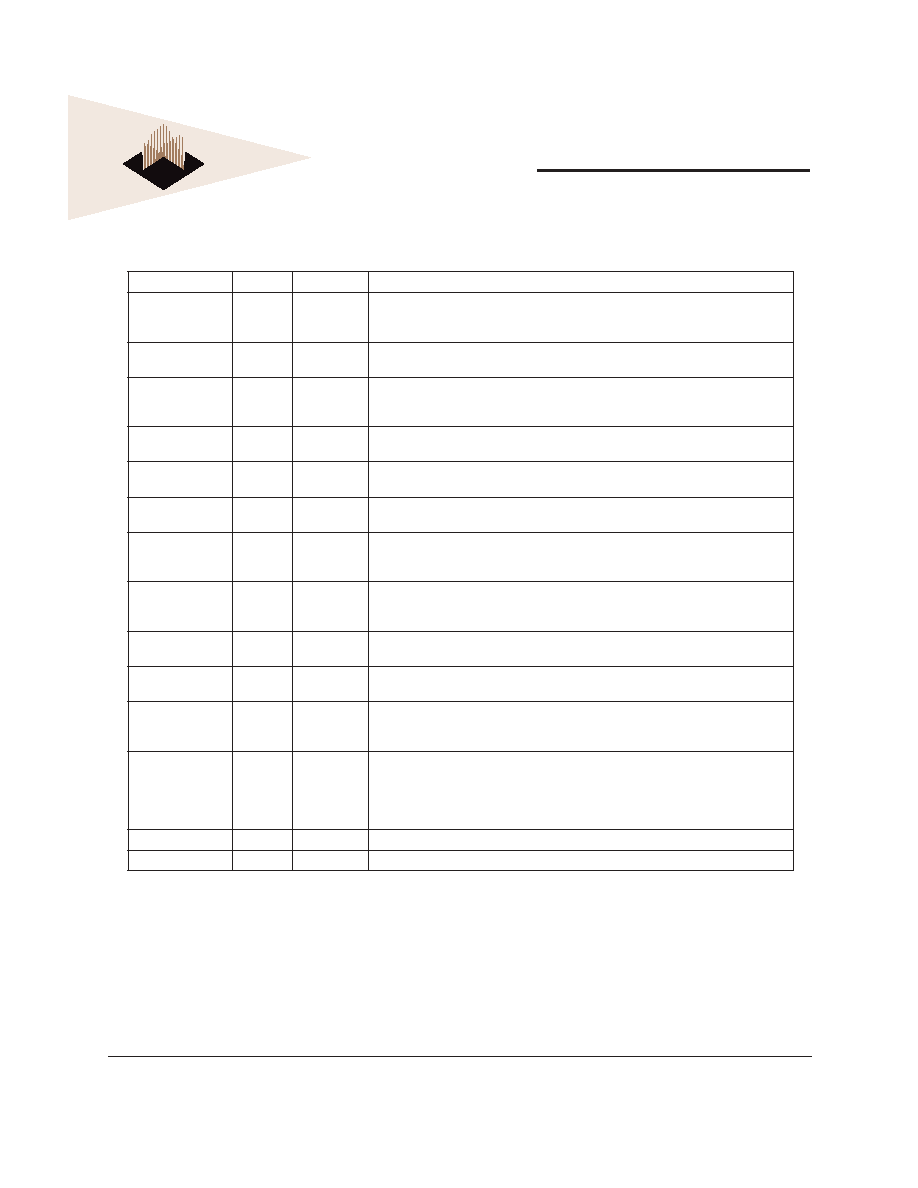
SYNCHRONOUS BURST - TRUTH TABLE
Operation
E1#
E2#
ADSP#
ADSC#
ADV#
GW#
G#
CK
DQ
Addr. Used
Deselected Cycle, Power Down; Bank 1
H
X
X
L
X
X
X
L-H
High-Z
None
Deselected Cycle, Power Down; Bank 2
X
H
X
L
X
X
X
L-H
High-Z
None
Read Cycle, Begin Burst; Bank 1
L
H
L
X
X
X
L
L-H
Q
External
Read Cycle, Begin Burst; Bank 1
L
H
L
X
X
X
H
L-H
High-Z
External
Read Cycle, Begin Burst; Bank 2
H
L
L
X
X
X
L
L-H
Q
External
Read Cycle, Begin Burst; Bank 2
H
L
L
X
X
X
H
L-H
High-Z
External
Write Cycle, Begin Burst; Bank 1
L
H
H
L
X
L
X
L-H
D
External
Write Cycle, Begin Burst; Bank 2
H
L
H
L
X
L
X
L-H
D
External
Read Cycle, Begin Burst; Bank 1
L
H
H
L
X
H
L
L-H
Q
External
Read Cycle, Begin Burst; Bank 1
L
H
H
L
X
H
H
L-H
High-Z
External
Read Cycle, Begin Burst; Bank 2
H
L
H
L
X
H
L
L-H
Q
External
Read Cycle, Begin Burst; Bank 2
H
L
H
L
X
H
H
L-H
High-Z
External
Read Cycle, Continue Burst; Bank 1
X
H
X
H
L
H
L
L-H
Q
Next
Read Cycle, Continue Burst; Bank 1
X
H
X
H
L
H
H
L-H
High-Z
Next
Read Cycle, Continue Burst; Bank 2
H
X
X
H
L
H
L
L-H
Q
Next
Read Cycle, Continue Burst; Bank 2
H
X
X
H
L
H
H
L-H
High-Z
Next
Read Cycle, Continue Burst; Bank 1
H
H
X
H
L
H
L
L-H
Q
Next
Read Cycle, Continue Burst; Bank 1
H
H
X
H
L
H
H
L-H
High-Z
Next
Read Cycle, Continue Burst; Bank 2
H
H
X
H
L
H
L
L-H
Q
Next
Read Cycle, Continue Burst; Bank 2
H
H
X
H
L
H
H
L-H
High-Z
Next
Write Cycle, Continue Burst; Bank 1
X
H
H
H
L
L
X
L-H
D
Next
Write Cycle, Continue Burst; Bank 1
H
H
X
H
L
L
X
L-H
D
Next
Write Cycle, Continue Burst; Bank 2
H
X
H
H
L
L
X
L-H
D
Next
Write Cycle, Continue Burst; Bank 2
H
H
X
H
L
L
X
L-H
D
Next
Read Cycle, Suspend Burst; Bank 1
X
H
H
H
H
H
L
L-H
Q
Current
Read Cycle, Suspend Burst; Bank 1
X
H
H
H
H
H
H
L-H
High-Z
Cur rent
Read Cycle, Suspend Burst; Bank 2
H
X
H
H
H
H
L
L-H
Q
Current
Read Cycle, Suspend Burst; Bank 2
H
X
H
H
H
H
H
L-H
High-Z
Cur rent
Read Cycle, Suspend Burst; Bank 1
H
H
X
H
H
H
L
L-H
Q
Current
Read Cycle, Suspend Burst; Bank 1
H
H
X
H
H
H
H
L-H
High-Z
Cur rent
Read Cycle, Suspend Burst; Bank 2
H
H
X
H
H
H
L
L-H
Q
Current
Read Cycle, Suspend Burst; Bank 2
H
H
X
H
H
H
H
L-H
High-Z
Cur rent
Write Cycle, Suspend Burst; Bank 1
X
H
H
H
H
L
X
L-H
D
Current
Write Cycle, Suspend Burst; Bank 1
H
H
X
H
H
L
X
L-H
D
Current
Write Cycle, Suspend Burst; Bank 2
H
X
H
H
H
L
X
L-H
D
Current
Write Cycle, Suspend Burst; Bank 2
H
H
X
H
H
L
X
L-H
D
Current